Where Should the Intelligence of the Network Be Placed: NIC, Switch, or xPU
DatenLord Tech Frontier Sharing NO.34
Time: 10:30 AM, September 17, 2023
As the performance of data center networks improves, offloading network-related tasks to smart NICs and smart switches has become a trend. At the same time, high-speed direct networks between GPUs, NPUs, and storage devices have also become a trend, where there seems to be no place for smart NICs. So where should the intelligence of the network be placed?
- Slides PPTX (32 MB)
- Slides PDF (15 MB)
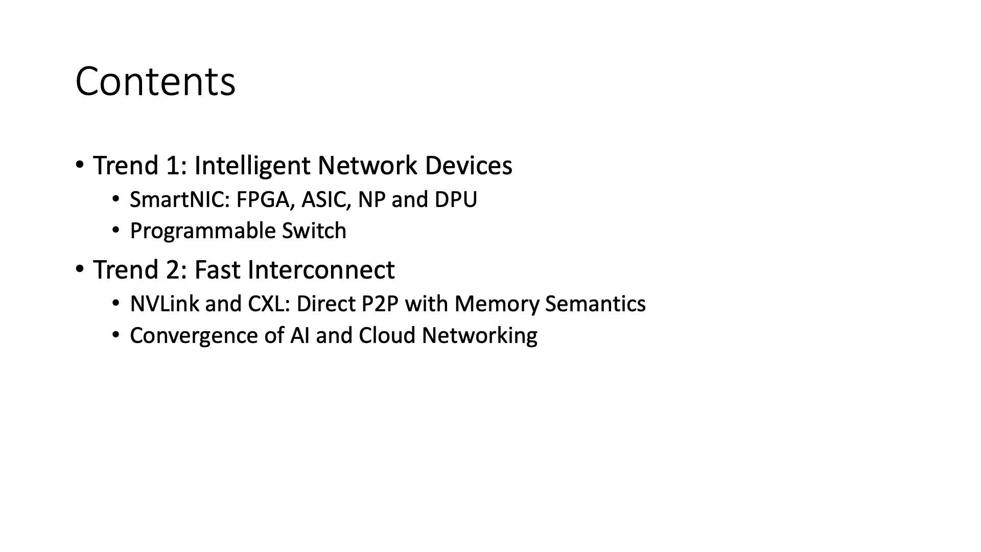
Below is a graphic record of the speech content, mainly organized by AI, and I made some manual corrections.

Thank you all for attending this frontier technology sharing event on the weekend. First of all, I want to thank Mr. Wang for his invitation, which gave me the opportunity to come to DatenLord to give this report. Today I will share some of my thoughts on network intelligence, including smart NICs, smart switches, and high-speed interconnect networks, etc.

First, I will briefly introduce some smart NICs and smart network devices, including programmable switches, as well as their current architecture and usage. Next, I will talk about our Fast Interconnect, that is, high-speed network interconnection, including content like NVLink and CXL, as well as some of our future development directions.
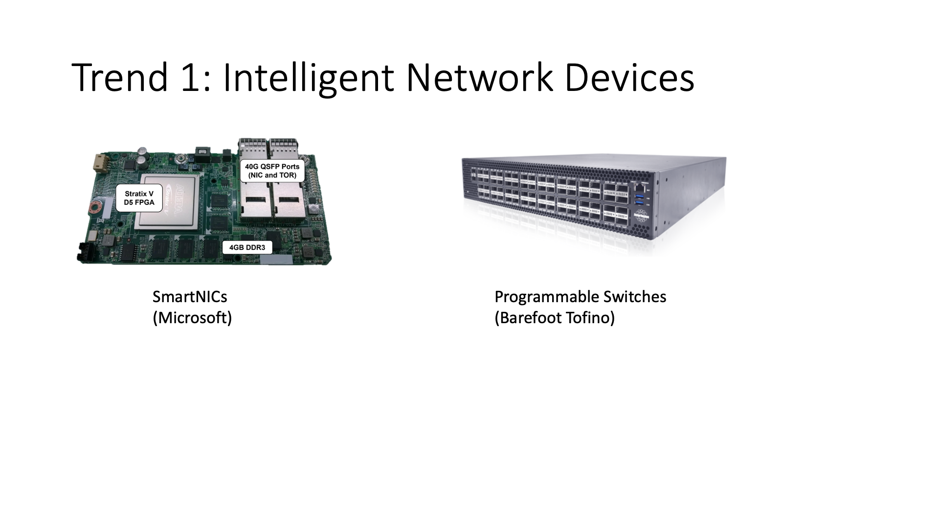
First, let’s briefly introduce some smart network devices. Smart network devices actually include two types, the first type is smart NICs, and the second type is programmable switches.
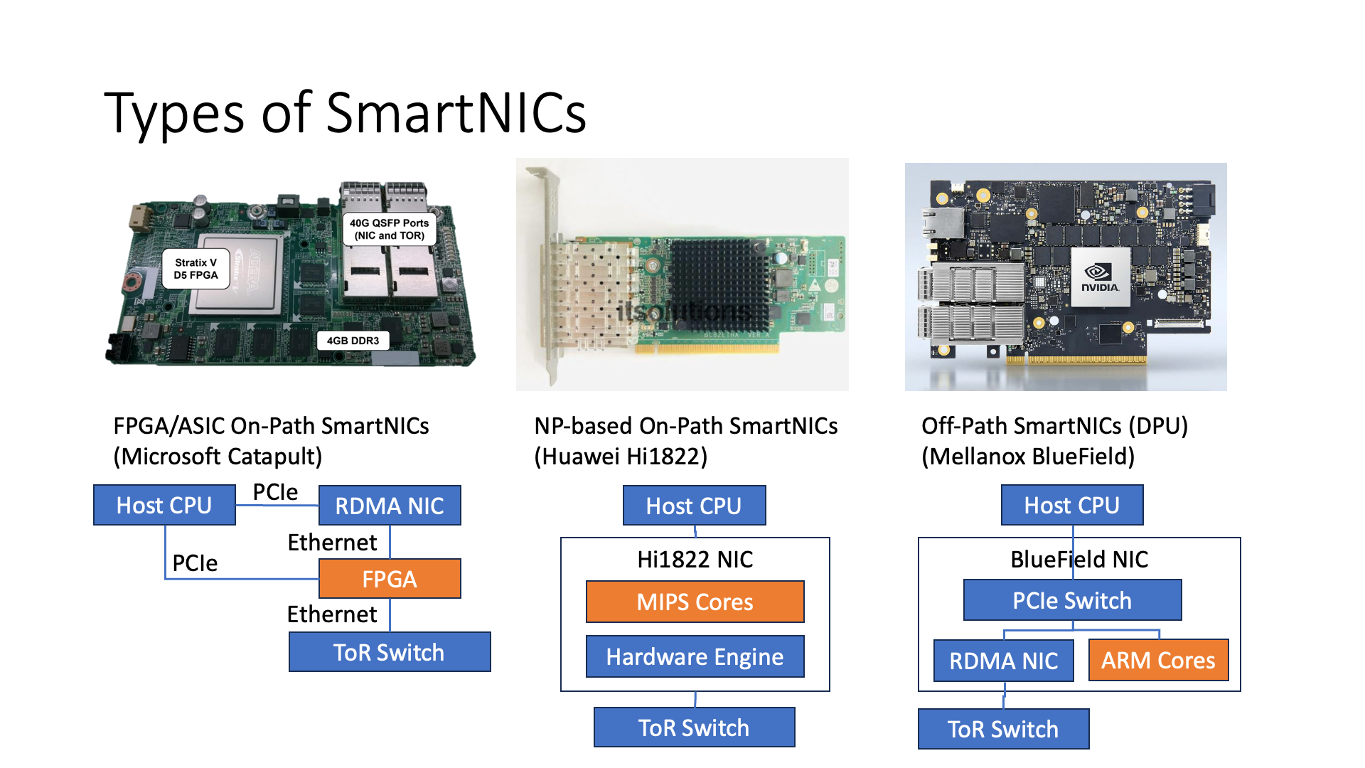
In the types of smart NICs, it can be roughly divided into three types. The first type is On-path SmartNIC based on FPGA or ASIC. The second type is On-path SmartNIC based on Network Processor. The third type is Off-path SmartNIC. So, what are On-path and Off-path?
In fact, we can see from this picture that the FPGA on the far left is actually on the necessary path of the network, that is, every network packet has to go through the intelligent processing part of the smart NIC, so this is called On-path.
For example, Huawei’s 1822 NIC, which is also a kind of NP (Network Processor). It also means that every time it processes a packet, it has to go through these programmable cores for processing.
But for example, Mellanox’s BlueField smart NIC, it belongs to another type of Off-path SmartNIC. What is Off-path? It means that these CPU cores are not on a critical path of network processing, which means that if I want to send some packets, for example, if the CPU directly calls the DMA interface to send, then it directly goes this way on the left, it will not go to the ARM on the right.
But if I want to do DMA, for example, I want to access a piece of memory on the Host CPU, it has to go this way and come back, or if I want to access other Hosts outside through RDMA, it can also go through this path on the left to access the outside Host, which means it is like an external attachment.
Next, I will introduce these types of smart NICs separately.
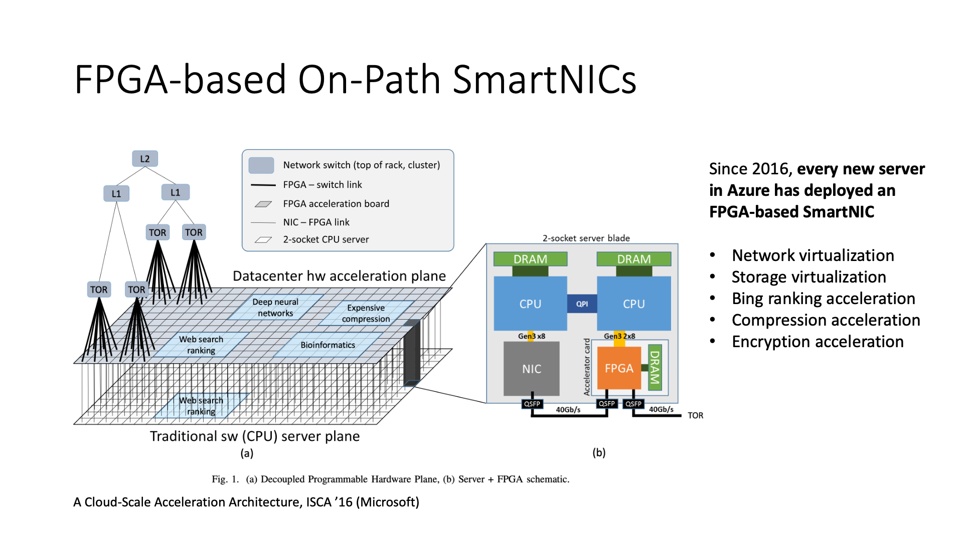
First of all, the most famous FPGA is actually Microsoft’s Catapult, and I have also done several years of research related to Catapult at Microsoft.
In fact, there are many companies in China now, such as Tencent, which are also using FPGAs to make Bare Metal machines. The so-called Bare Metal means that this machine can be used as a whole, and then sold directly to you, you can install any system on it, but I can still ensure its security and isolation, why?
Because there is a card outside, equivalent to the CPU part of the thing is actually the customer can control, but the NIC and FPGA part of the thing, is managed by our Infrastructure.
Microsoft was not originally using FPGA to do network virtualization, it was originally used to accelerate Bing search, because there is a process of search result ranking in Bing search, in the process of ranking, it actually mainly uses some deep neural network things, so it put some neural network things on the FPGA to do some acceleration, the scale of deployment at that time was not particularly large, just over 1000 cards.
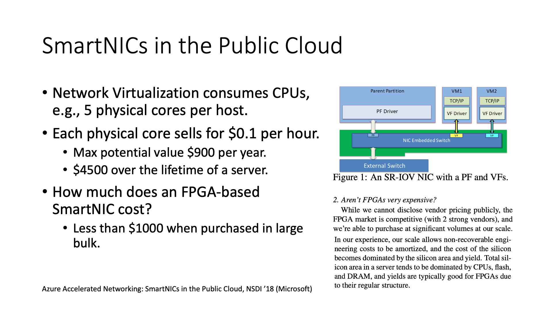
The scale of the story grew later. Doug Burger, the person in charge of Microsoft’s FPGA, said that he wanted to deploy an FPGA on every machine in the entire data center. What for? It is used for Network Virtualization, because we know that network virtualization requires a lot of resources. So if we only use our CPU for network virtualization, it may need 5 physical CPU cores per Host. If you do the math, it might be said that the entire lifecycle of the entire Host is equivalent to a loss of 4500 US dollars. Of course, this is calculated at the maximum, meaning that if all the CPUs on all the Hosts are sold out, then he will lose so much.
So how much overhead will it bring if I add an FPGA smart network card? This FPGA is definitely expensive if it is retail, that is, an FPGA is over 1000 US dollars.
But this FPGA first of all does not use the highest-end FPGA. At that time, it was always one generation lower than the highest-end FPGA, because network virtualization does not require such high computing power, as long as it is enough.
The second is because Microsoft’s scale is particularly large, such as millions of FPGAs. From the screenshot of this paper, you can see that when the scale is large enough, the design cost of the chip can be spread out, so the price of the chip is basically proportional to the area of the chip under the same process. So the price of an FPGA is actually just over 200 US dollars, plus our RDMA network card is over 200 US dollars, and then add the DRAM just mentioned, and the cost of the circuit board, the overall cost is actually less than 1000 US dollars.
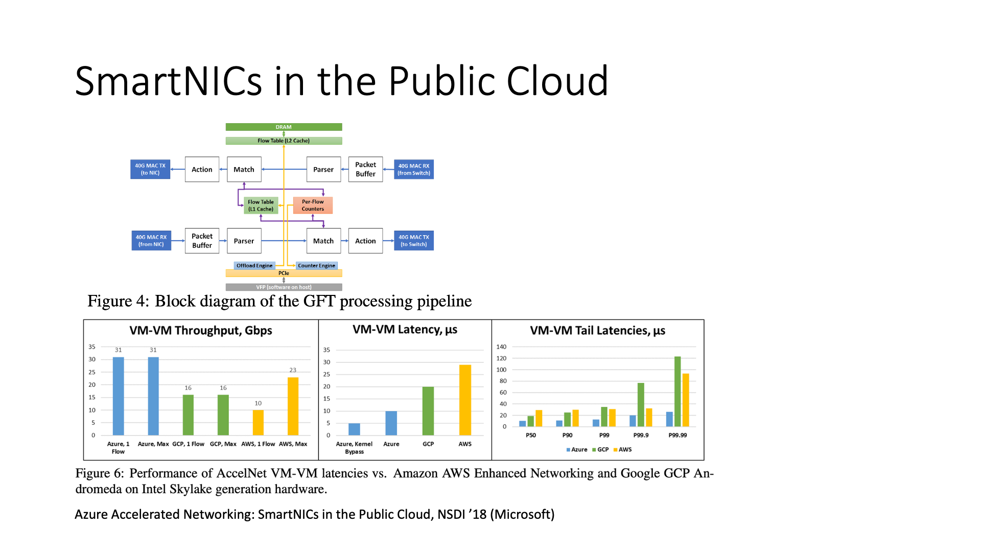
Under these circumstances, large-scale deployment of FPGA becomes possible. Microsoft used FPGA to build a network virtualization processing pipeline, which is called GFT (Generic Flow Table). It can be understood as a lookup table, which contains some rules, and the messages are matched and processed according to these rules, which is equivalent to integrating the flow table into the FPGA.
Because the flow table method is used, we do not need to frequently re-burn the FPGA, and only need to modify the flow table when the rules change.
Using this method, I can greatly shorten the latency from VM to VM, and greatly increase the throughput. This is a classic paper published by Microsoft in 2018.
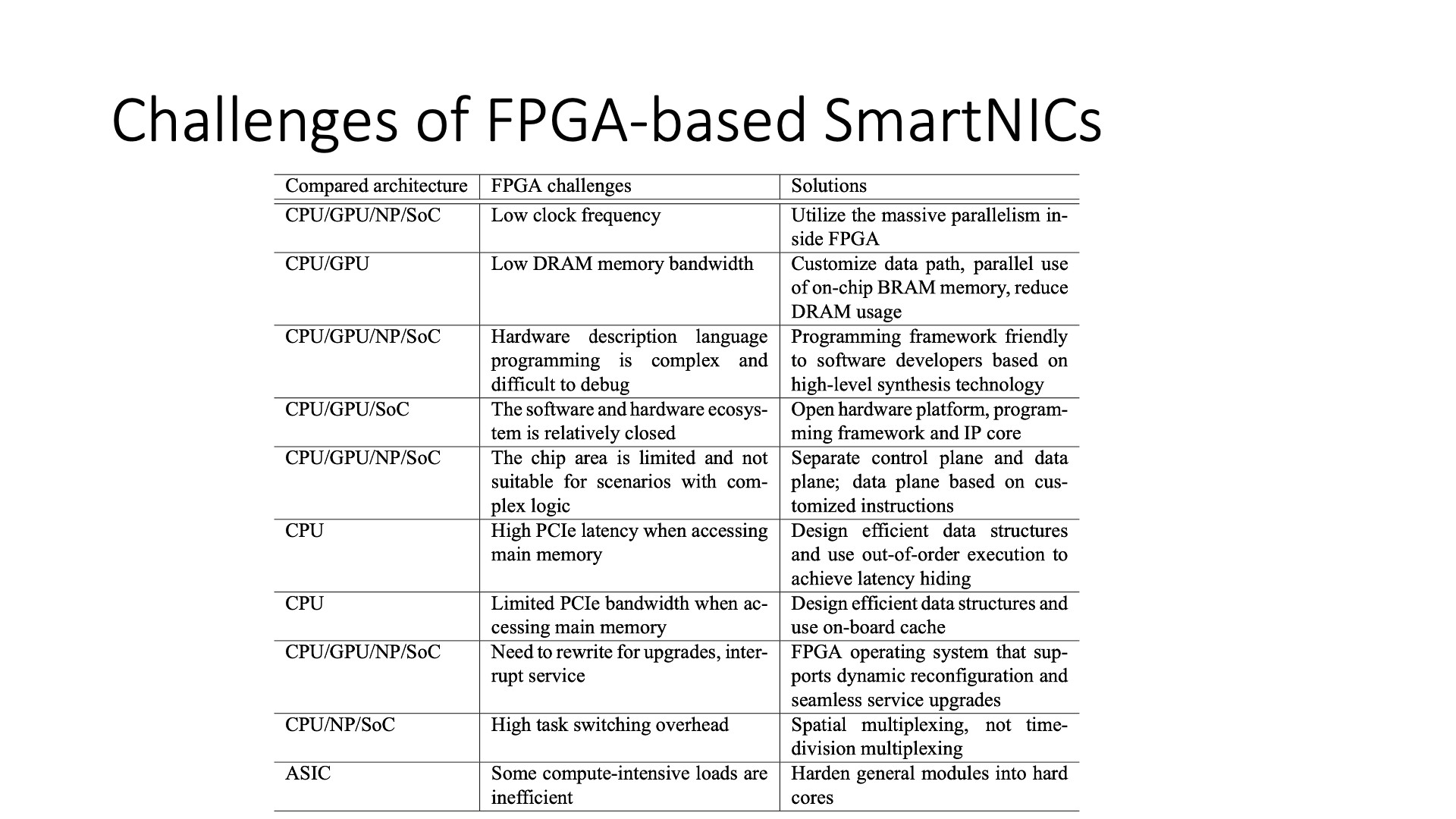
However, there are still some problems with FPGA, such as the difficulty of programming is relatively large, and ordinary software engineers may not be able to write. In addition, because its chip area is small, it cannot accommodate complex logic, so we can only put the content of the data plane into it, and the content of the control plane should still be kept on the CPU for processing.
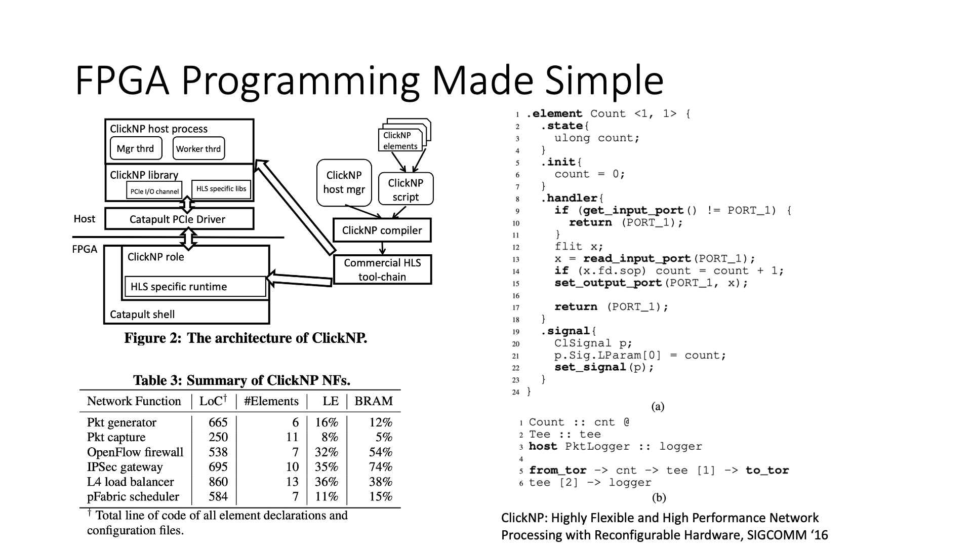
We have done a research work to make FPGA programming simpler, and can use C language programming, without using Verilog. We developed a compiler, using HLS tools, which can compile OpenCL into FPGA logic. However, because OpenCL’s compilation ability is weak, we developed a framework on it, which can translate the network processing language we defined into more efficient OpenCL language, and then use HLS tools to generate FPGA logic. This is also a paper we published before.
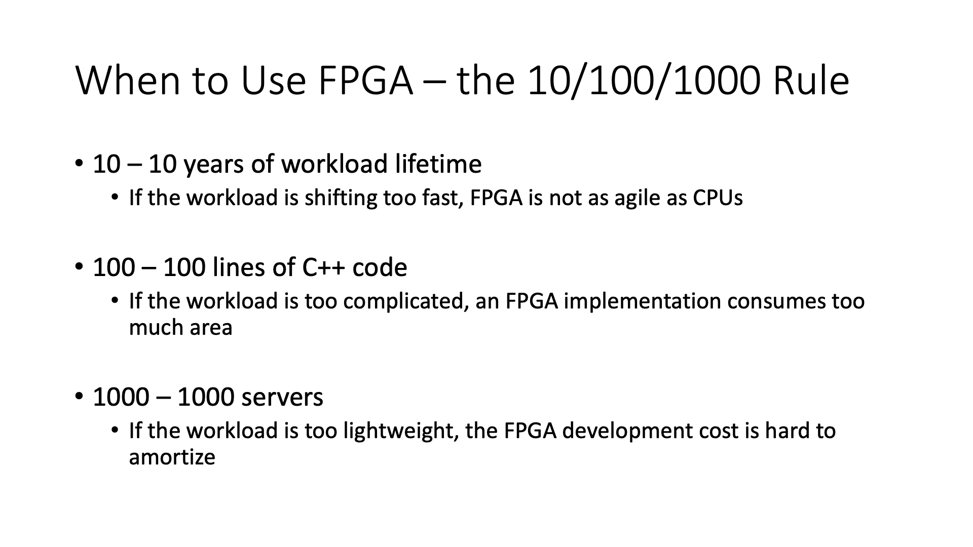
We summarized it, under what circumstances it is more appropriate to use FPGA, it is a 10-100-1000 rule.
First of all, the workload needs to be used for 10 years, which means that if this workload may be used for one year this year, and then not used later, then the cost of FPGA development is actually very high. And FPGA development is not particularly agile, the FPGA development cycle is long, and it is not easy to develop, and the demand may change.
Secondly, 100 lines of code, which means that if you write in a high-level language, you may need to write 10,000 lines of code, which may not fit on the FPGA, because the size of the logic gate on the FPGA is actually limited. This is not to say the number of lines of Verilog code, maybe 100 lines of C++ code need to be translated into tens of thousands of lines of code in Verilog.
Finally, 1000 servers, which means that if this service doesn’t need many machines, for example, it is a very small workload, at most 100, then I really just buy 100 CPU servers, and there is no need to think about using FPGA to accelerate. If there are too few servers, it is not worth developing FPGA.
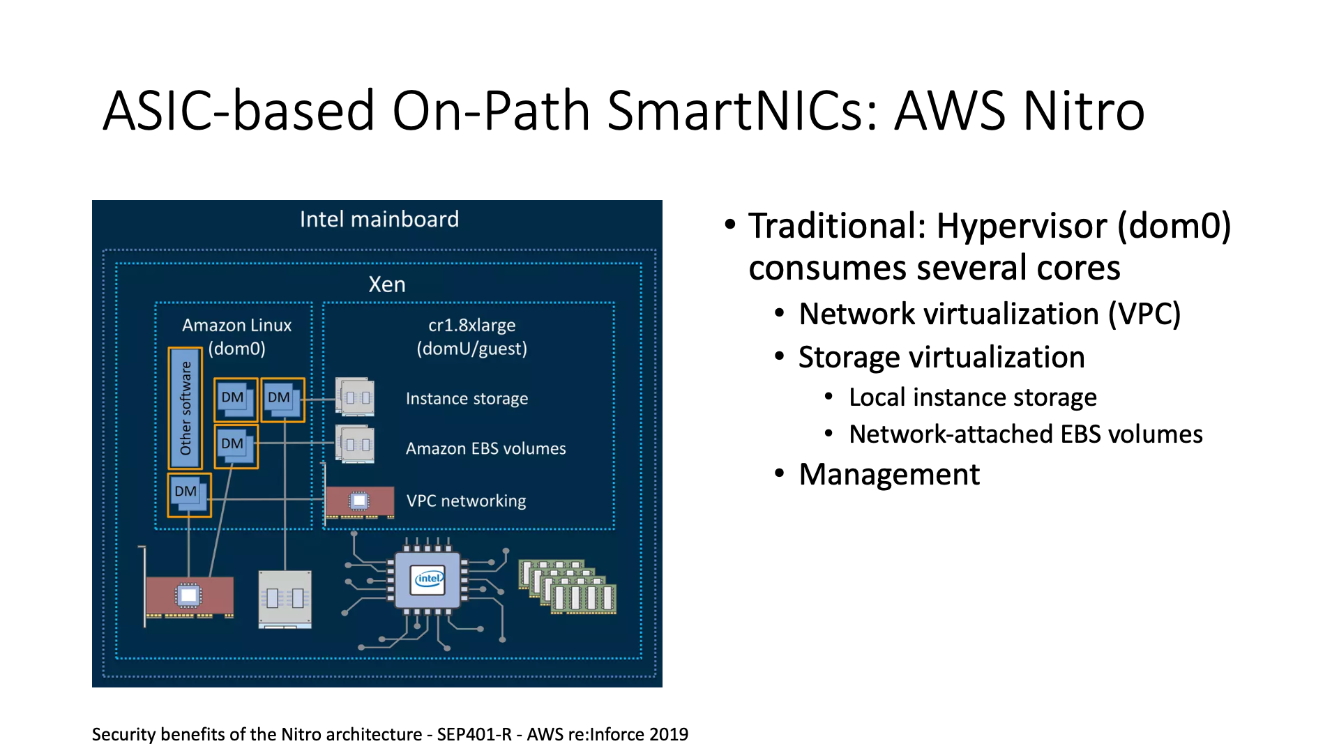
In fact, FPGA development and ASIC development are similar to some extent. For example, Microsoft Azure’s biggest competitor AWS, they use the self-developed ASIC-based Nitro card. From an architectural point of view, they are basically the same, just choosing different technical paths. Microsoft chose FPGA, while AWS chose ASIC, also to save the overhead of network, storage virtualization and management.
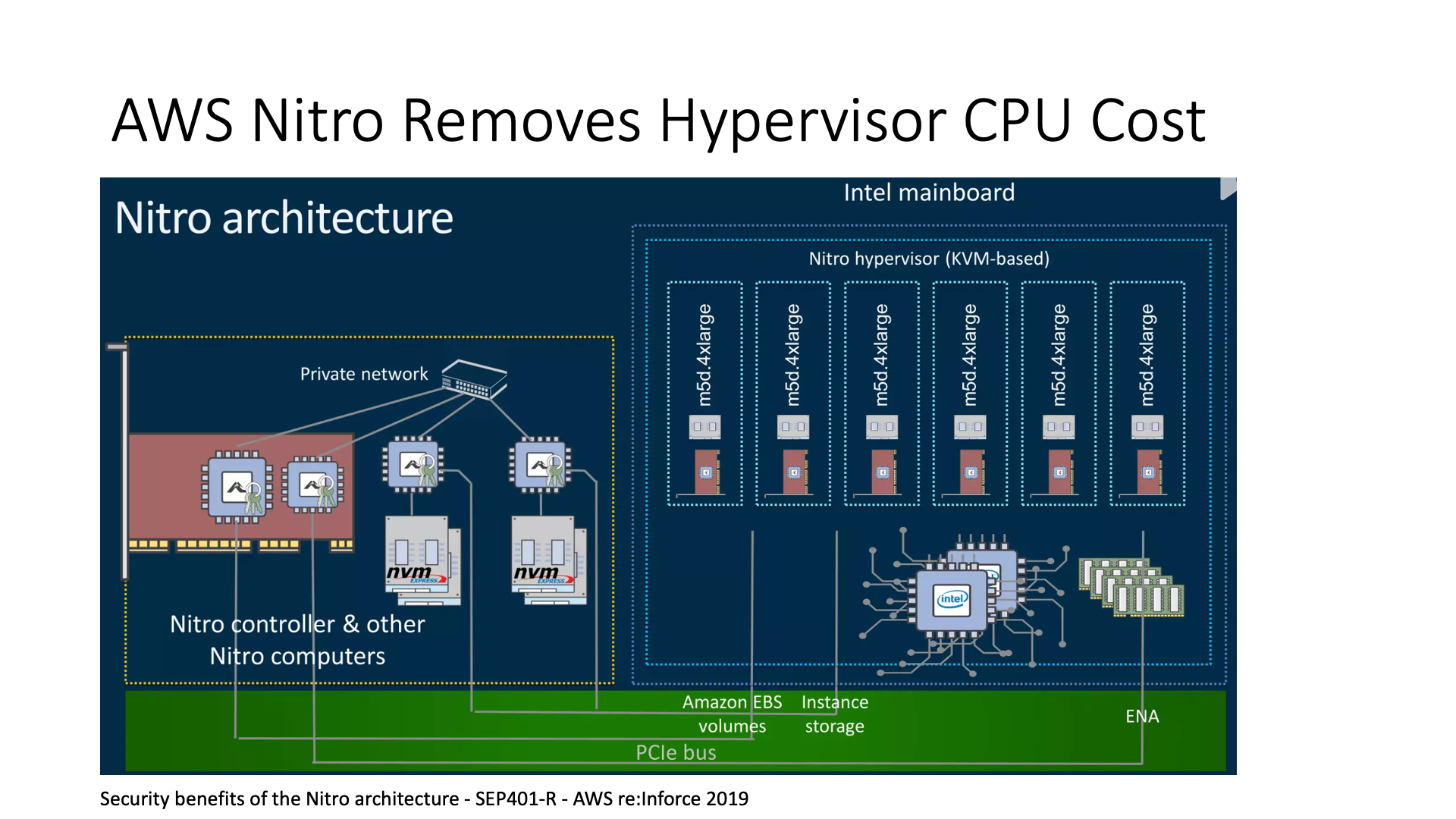
AWS’s approach is to offload the content originally processed on the CPU to their smart network card. The smart network card is actually mainly an ASIC-based card, which can be understood as the code we used to write on the FPGA, that is, Verilog, they burned it into ASIC.
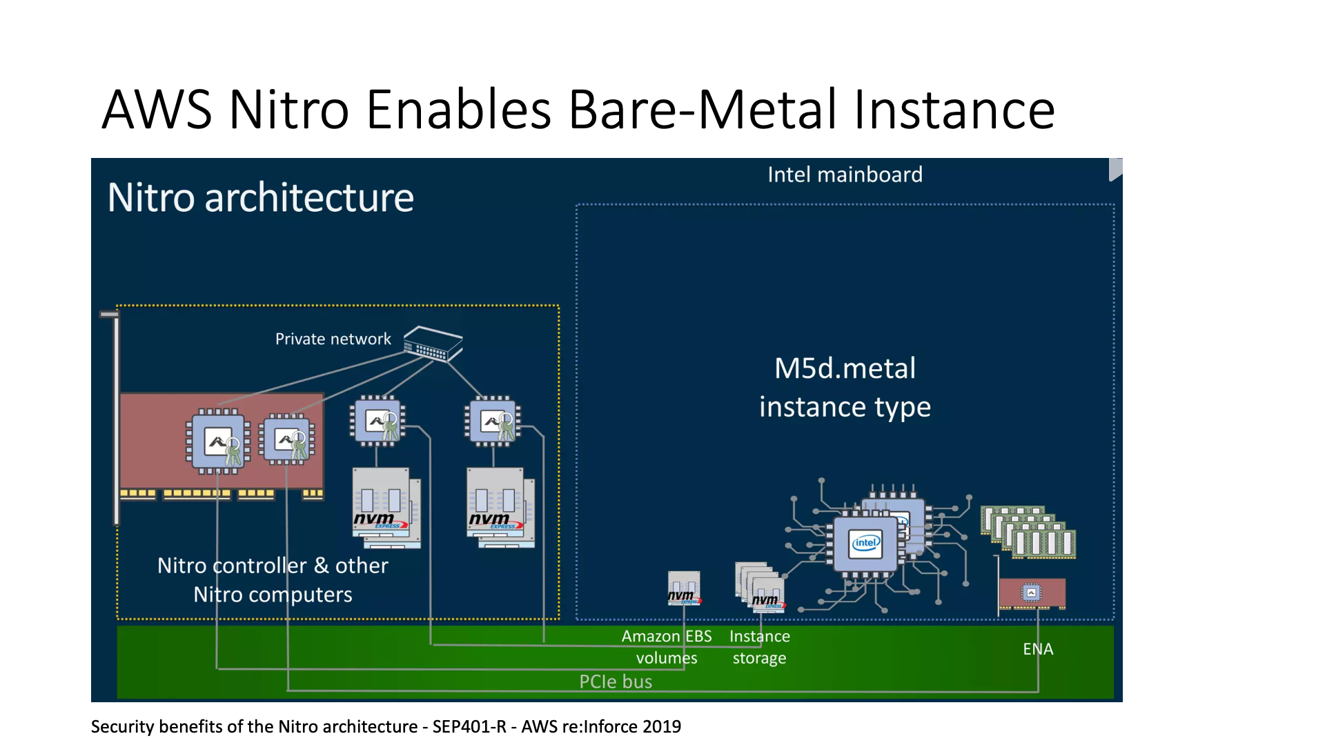
AWS has also developed a Bare Metal Instance. Tencent’s Bare Metal uses a smart network card based on FPGA, and Microsoft and AWS’s Bare Metal also use the method of smart network cards, but the internal architecture of the network card is different. Without this card, it is actually difficult to implement Bare Metal because you need to add an extra machine to manage it.
For example, Bare Metal machines definitely need to mount shared storage or network disks in the cloud, and I can’t let it directly access the network, which is too dangerous, so there must be someone watching it outside. How to manage these things is actually the job of the smart network card. Now I just need to plug this smart network card into this machine, and then this machine can be sold as a whole.
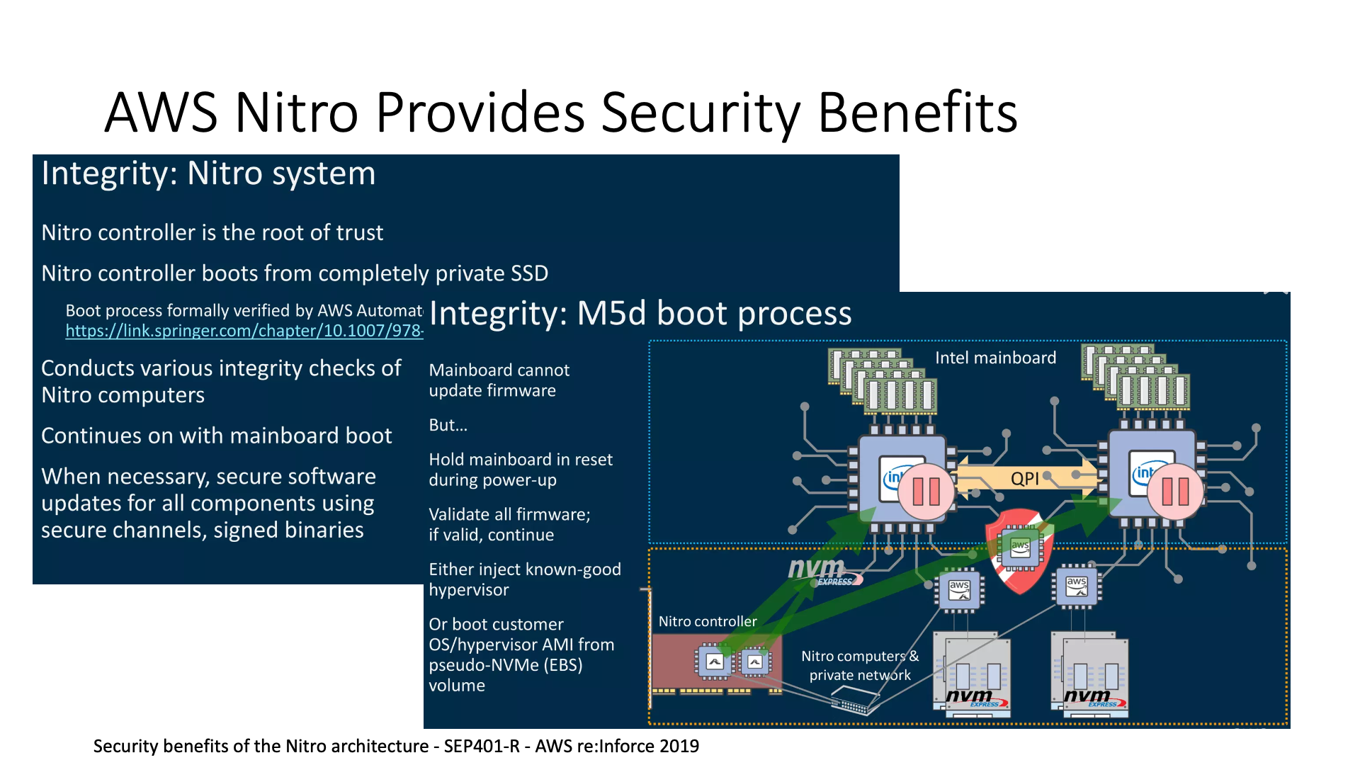
At the same time, like Nitro, and the Catapult FPGA we mentioned earlier, they all provide some security advantages. We can use it as a trusted root, which means that traditional trusted roots come from the CPU. I install a boot loader on the CPU, and then layout as a trusted root on the boot loader, but there is a problem here. What if the raw access of the disk is broken and the boot loader is modified? This situation is quite dangerous.
In the architecture of AWS Nitro, it puts the root of trust in the smart network card controller, so users can directly access and manage the entire disk without worrying about other problems.
Nitro also provides a security check function, during the startup process, it can also check the firmware of various devices of the entire machine.
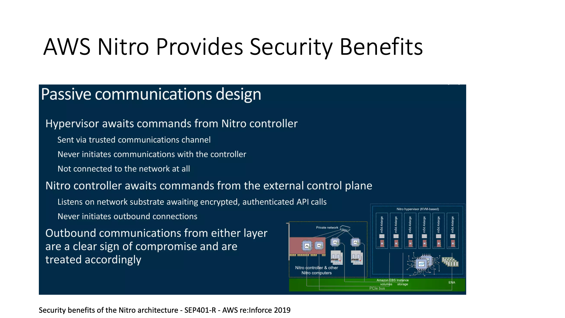
In addition, Nitro has also implemented a kind of passive communication. The traditional communication mode may be that the machine actively initiates a connection, possibly attacking the controller, or directly initiating a connection to the Internet or other hosts in the cloud, sending sensitive data out.
However, the existence of the smart network card (SmartNIC) has changed this situation. Because this card is in the host, it establishes a long connection with the host’s Hypervisor, and then the smart network card establishes a long connection with the external control plane. In this way, it no longer needs to actively initiate a connection, this behavior can be directly prohibited at the network level, that is, on the switch. This can prevent the problem of actively initiating a connection to send information out after the Trojan is injected, which is a point of enhanced security.
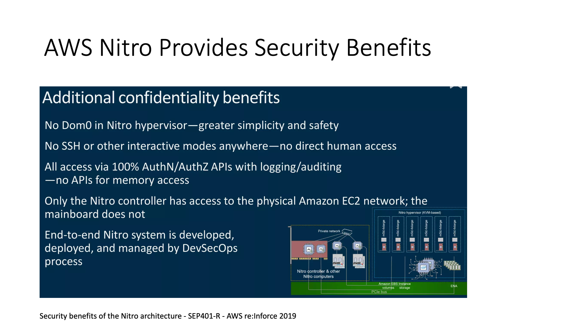
Of course, Nitro also has some other functions, such as it can move the functions originally in the virtual machine (VM), because the original Hypervisor’s Dom0 needs at least one CPU core, and then move this CPU core to the smart network card, so that it can have higher security, and can also save the cost of the CPU core.
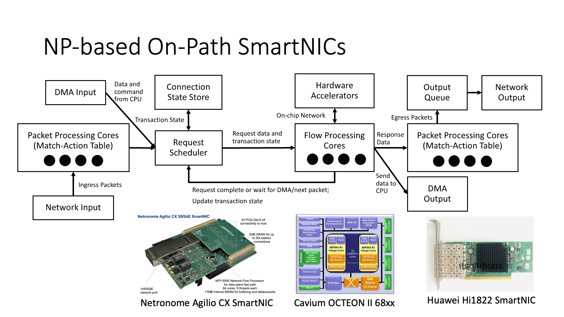
Next, let’s introduce another type of smart network card. The previous introduction was based on FPGA or ASIC. What we are introducing now is based on network processors. This is also a very typical type of smart network card. For example, there are Netronome, Cavium, and Huawei’s 1822 smart network cards. They all have similar architectures, with some small MIPS cores or ARM cores inside for data processing.
The places on the far left and far right of the picture that say packet processing core are not actually general-purpose CPU cores, but some match action tables. This table is a bit like the Microsoft GFT (Generic Flow Table) we mentioned earlier.
In the middle of the picture, there are also some flow processing cores. This is the real ARM or MIPS core. It is actually used to do some logical processing. For example, in the RDMA card, the entire RDMA (Remote Direct Memory Access) engine is mostly implemented by the flow processing core, and it is not the RDMA protocol that is hardcoded.
What are the benefits of this? For example, if I want to update its congestion control algorithm, I can directly change the code inside this flow processing core, and then the congestion control algorithm is changed. Or if I want to upgrade the protocol to be compatible with other cards, such as Mellanox’s card, I can also change my code, which makes development more agile. This is the same reason as FPGA.
Network Processor (NP) programming seems to be based on general processor cores, but it is not a general processor, there is no operating system on it, so the code on NP is not software on a general CPU, but is generally referred to as microcode. It is not much simpler than FPGA, it is actually quite complex.
Because we see that this stream processing core is not a simple external CPU, but is connected to many hardware structures. For example, it is connected to a hardware accelerator. If I want to add a message header to the packet, I don’t write a memcpy in the stream processing core, move all the contents behind the packet, and then add something on the head, which is definitely inefficient. The function of the hardware accelerator is that I directly insert the message header into the specified position, and the remaining memory moving work is done by hardware, which will be more efficient.
There is also a Connection State Table (QP Context Table), which stores the state of each connection. If we write a program on the CPU, how do we store its state? It must be to make an array or dictionary in the global variable. But think about it, if I make a dictionary on the stream processing core, and so many stream processing cores are going to access the dictionary concurrently, and also need to lock, the efficiency will definitely not be very high.
Therefore, NP still uses hardware to implement this state storage (state store), that is to say, the state of each of its connections is managed by hardware, and then I use the QP number to find it every time, and then schedule according to this, that is, the scheduling here is also done by hardware, that is, it is hardware scheduling instead of software scheduling, this is the most fundamental difference between NP and general CPU.
Why do we need to schedule hardware here?
We know that software scheduling actually has a big problem. Because we know that software scheduling can usually only handle one core, its scheduling ability is limited. If we have multiple cores, we can only balance the load, that is, we need to distribute the input data evenly to multiple cores according to certain conditions, and then process it. However, there is a problem here, that is, if a data stream is particularly large, such as a data stream may be 80 Gbps, and another is only 20 Gbps, they can only be assigned to different cores, a data stream can only run on one core, which leads to unfair scheduling.
However, if we use a hardware scheduler, whether it is on FPGA or NP, it can achieve more fair scheduling, because it is a hardware module, all data streams will pass through it, and then schedule, this is the difference between centralized scheduling and distributed scheduling.
But there are still some problems, if a data stream is particularly large, there will still be problems. Because if a data stream is very large, then between processing one packet and the next packet, its state needs to change constantly. So, if the previous packet is not finished, the next packet cannot be processed. So, at this time, a data stream can usually only be pipelined on one or a few cores. Then, in the pipeline, the number of cores is definitely limited, because it is a hardware pipeline, the depth is fixed.
Therefore, NP cannot schedule all cores to process packets on a stream. At this time, its single-stream performance will have some limitations. So, this is also its main difference from FPGA, because the pipeline of FPGA is programmable, complex logic can be unfolded in space instead of in time.
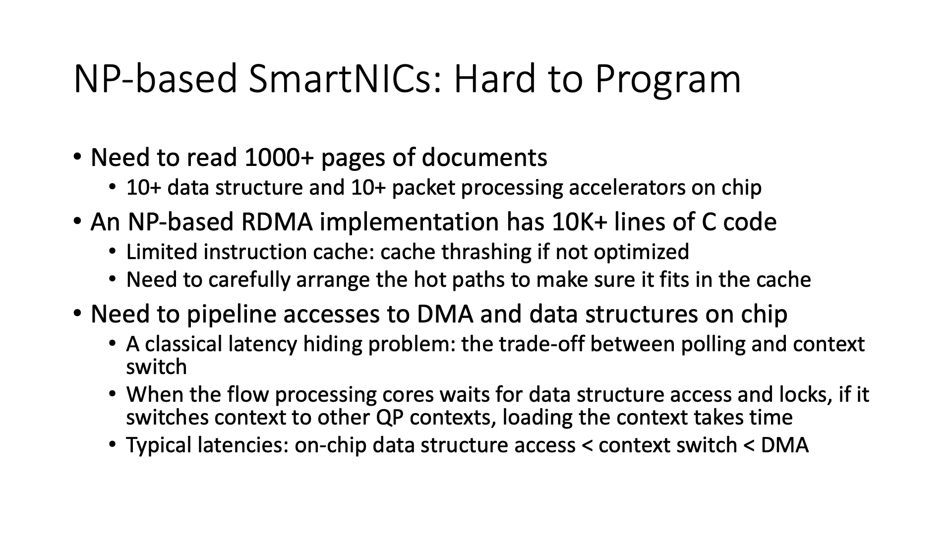
NP programming is actually not as simple as imagined, not because it has a CPU inside, it can be programmed casually. Its documentation is very complex, because the interfaces of various accelerators inside are different.
The code inside NP also needs to be pipelined. For example, I am going to access a data structure now, should I wait for it to access back, or should I switch to other tasks first, and then switch back when the access result comes back? This is a classic problem of polling and context switch. Because the on-chip data structure is usually very fast, so it is usually not worth doing context switch, usually wait for completion, or use hardware pipeline to cover it. Of course, if it is DMA (Direct Memory Access), it is slower, it is worth switching. The switch of QP Context may also be a problem without a good solution.
Of course, there are some other problems, such as the problem of instruction cache, that is, for example, I have 10,000 lines of C code. 10,000 lines of C code, if I make all of them into an NP-based implementation, it can be stuffed into the card’s memory, but the problem is that its cache can’t fit, which will also cause a big performance problem. Why is this more troublesome than on the CPU? It’s because the caches of general CPUs are larger, they are all in the megabytes, but the stream processing cores in NP are small cores, their caches are in the tens of KB. So you have to optimize the code on NP well, you need to arrange the frequently accessed hot path into the cache. This is also a problem brought about by its architectural limitations.
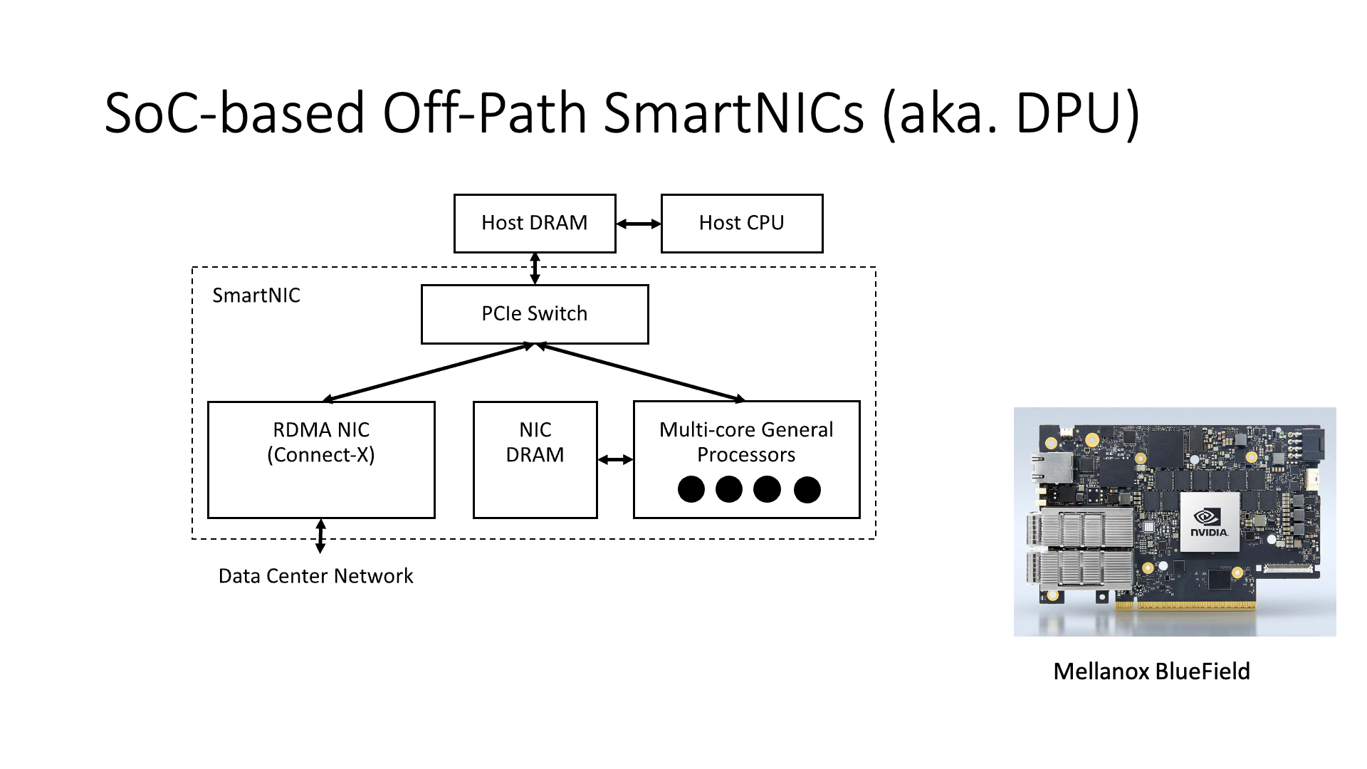
Like Mellanox, it takes another path, it says I have a few big cores, I won’t do this small core. The previous NP (Network Processor) architecture, its cores are usually small cores, they are some cores with relatively poor performance.
However, Mellanox’s BlueField card, for example, has 4~8 relatively large ARM cores. But this smart network card is actually a bit of a chicken rib if it only uses these few ARM cores, why? You see its architecture, it is actually an off-path. The previous architectures are all on-path, all processing on the necessary path of network packets. But in Mellanox BlueField, for example, on the host’s CPU, to send an RDMA request, it has nothing to do with the ARM core in the network card, because it goes directly to the network from the left network card part.
Then, if this ARM core wants to access the host memory on the CPU, well, it also has to access through the PCIe switch. In the old version of BlueField, it can’t even directly access the CPU, it needs to go through this NIC to access, that is, it didn’t initially make a channel for this ARM core to directly access the host memory. If you want to access, the ARM core first needs to access the network card through RDMA, and then the network card goes to access the host memory, so the entire latency is 1.6 microseconds upwards. The later BlueField 2 made the way for the ARM core to directly access the host memory, and at this time it only needs a few hundred nanoseconds to access the host memory through PCIe, which is much faster.
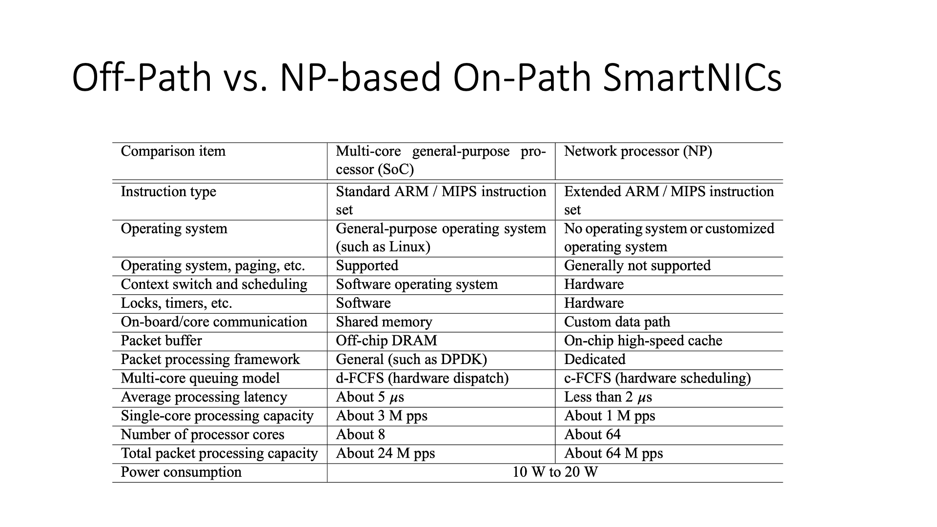
This is the architecture of the Mellanox BlueField Smart Network Card (SmartNIC). The main difference between its architecture and the network processor (NP) is that, first of all, there is a general operating system inside the smart network card, such as Linux. However, there is no operating system inside the network processor, that is, it needs to write microcode (Microcode).
Secondly, in terms of scheduling, etc., the efficiency of NP hardware is higher than that of external ARM cores. Although the stream processing core inside the NP has relatively poor performance, it has a performance of only about 1M pps, but 64 cores together have 64M pps. Although each ARM core can handle 3M pps, 8 cores together only have 24M pps. Therefore, the ARM cores in the Off-path SmartNIC cannot be used for large-scale tasks. If every packet has to go through it once, it can’t stand it. In addition, the processing latency of the ARM core is relatively long, which is the difference between 5 microseconds and 2 microseconds.
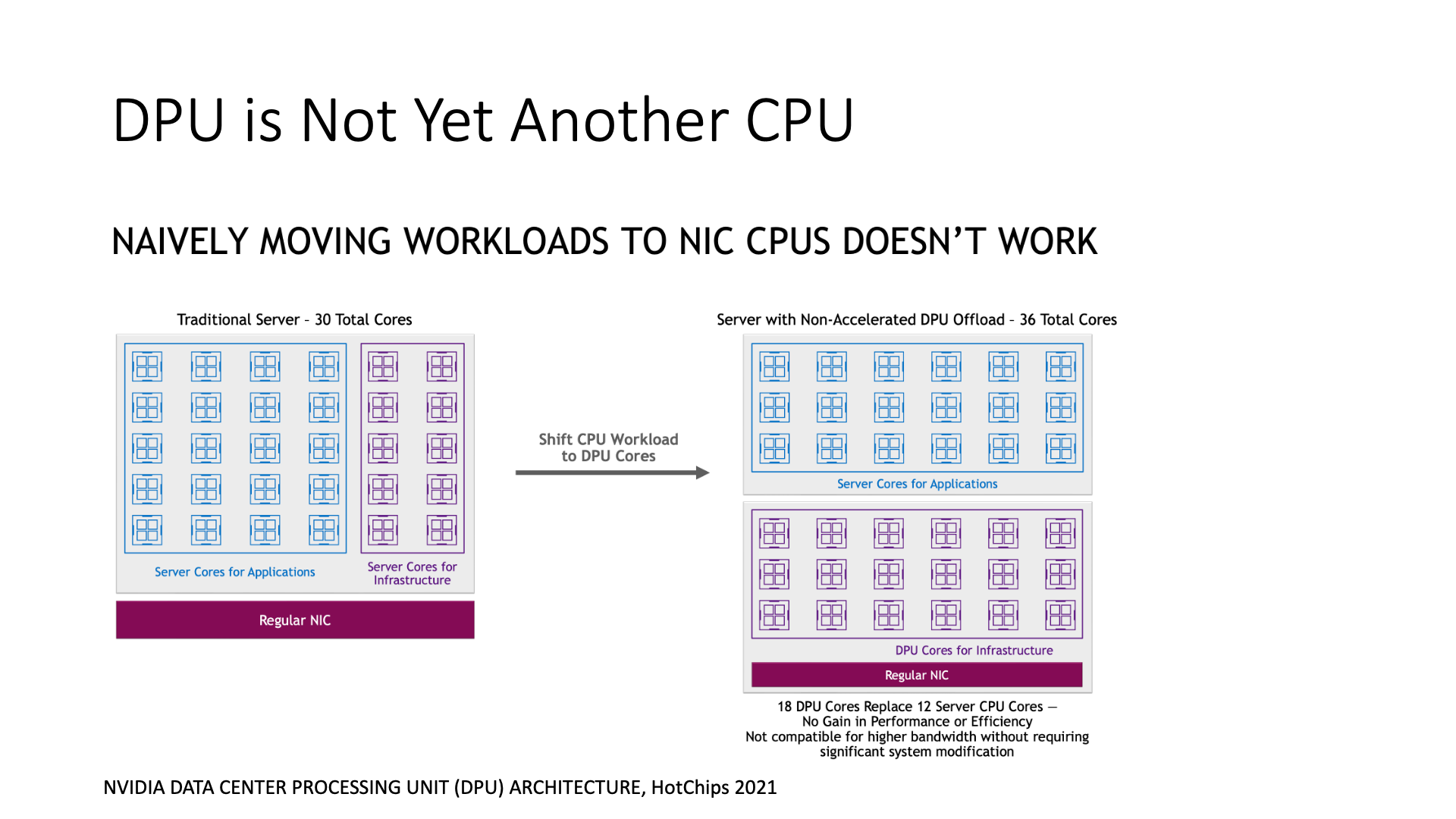
So we see that if a general operating system is running on the smart network card, it is just used as some external CPU cores for processing, then it is actually very chicken rib. NVIDIA also realized this problem, so they also proposed the DPU architecture. The DPU should not use its core as a regular CPU core, because the performance will definitely not be good.
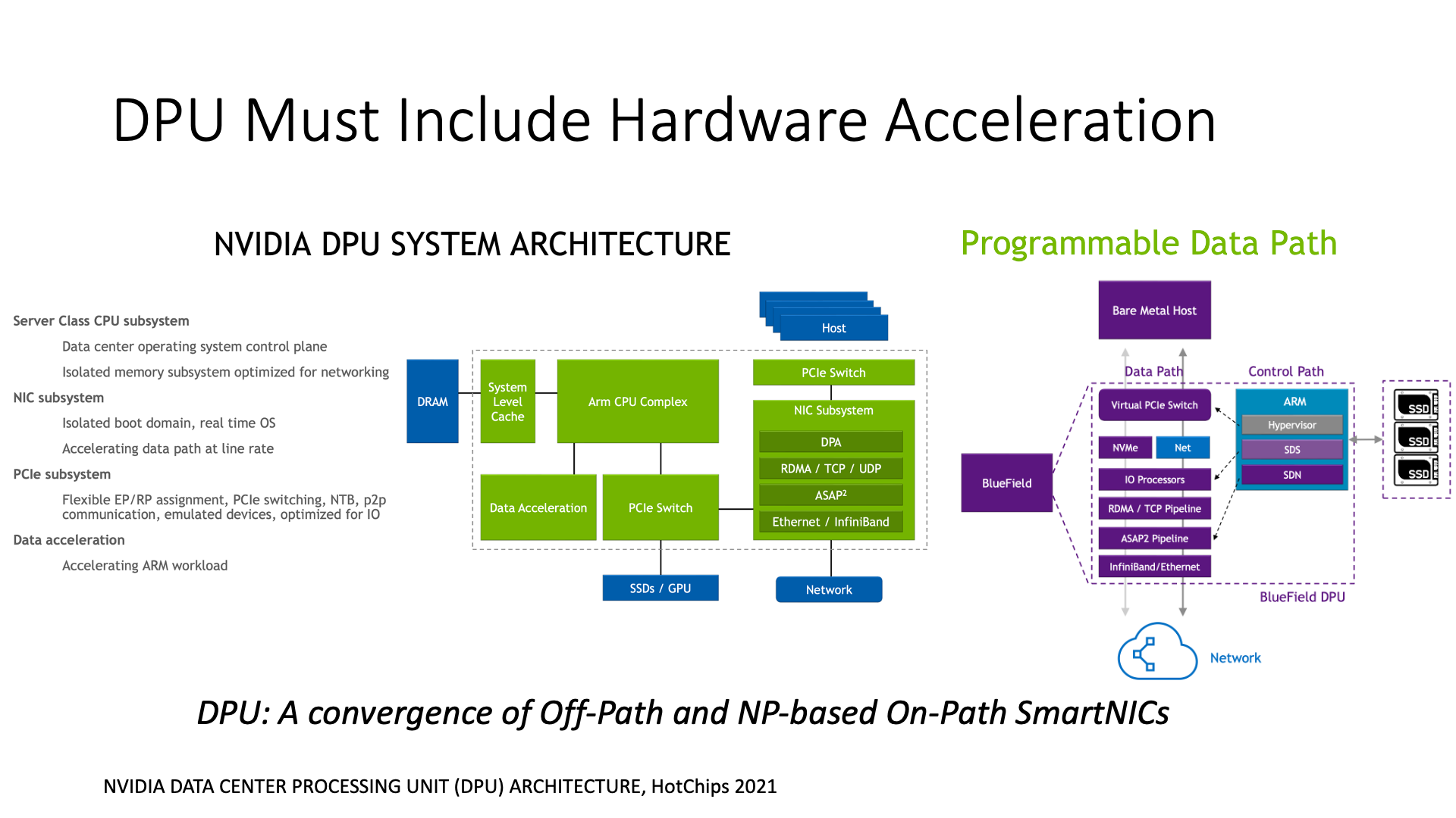
So it also needs to add some extensions, which is equivalent to the DPU absorbing some things from the architecture of the network processor. The architecture of the DPU is actually a combination of the Off-Path SmartNIC architecture and the network processor architecture.
First of all, it did not completely give up the concept of running an operating system on the smart network card, because this is very helpful for programmability. If a standard Linux can run on it, and then a DPDK can run on it, even if it is a customized version of DPDK, for users, those who are used to programming on Linux, they are very used to it. But if it is a network processor, unless you read that thousands of pages of documents, you basically can’t start programming. So programmability is different.
In order to improve performance, the DPU has added many engines, including ARM cores, and then it has added a hardware accelerator in these ARM cores, which is actually like a network processor, which puts hardware accelerated packet processing, encryption, compression and other functions here. Then the DPU also added some lookup table functions, which are also placed here.
BlueField also added a function that can directly connect to storage, which can directly mount some NVMe disks, and directly hang the disks on the BlueField network card. The reason for doing this is to facilitate storage virtualization. The previously mentioned cards like Netronome or Microsoft’s FPGA cards, they are all used for storage virtualization, and NVIDIA now also puts the function of storage virtualization on the DPU.
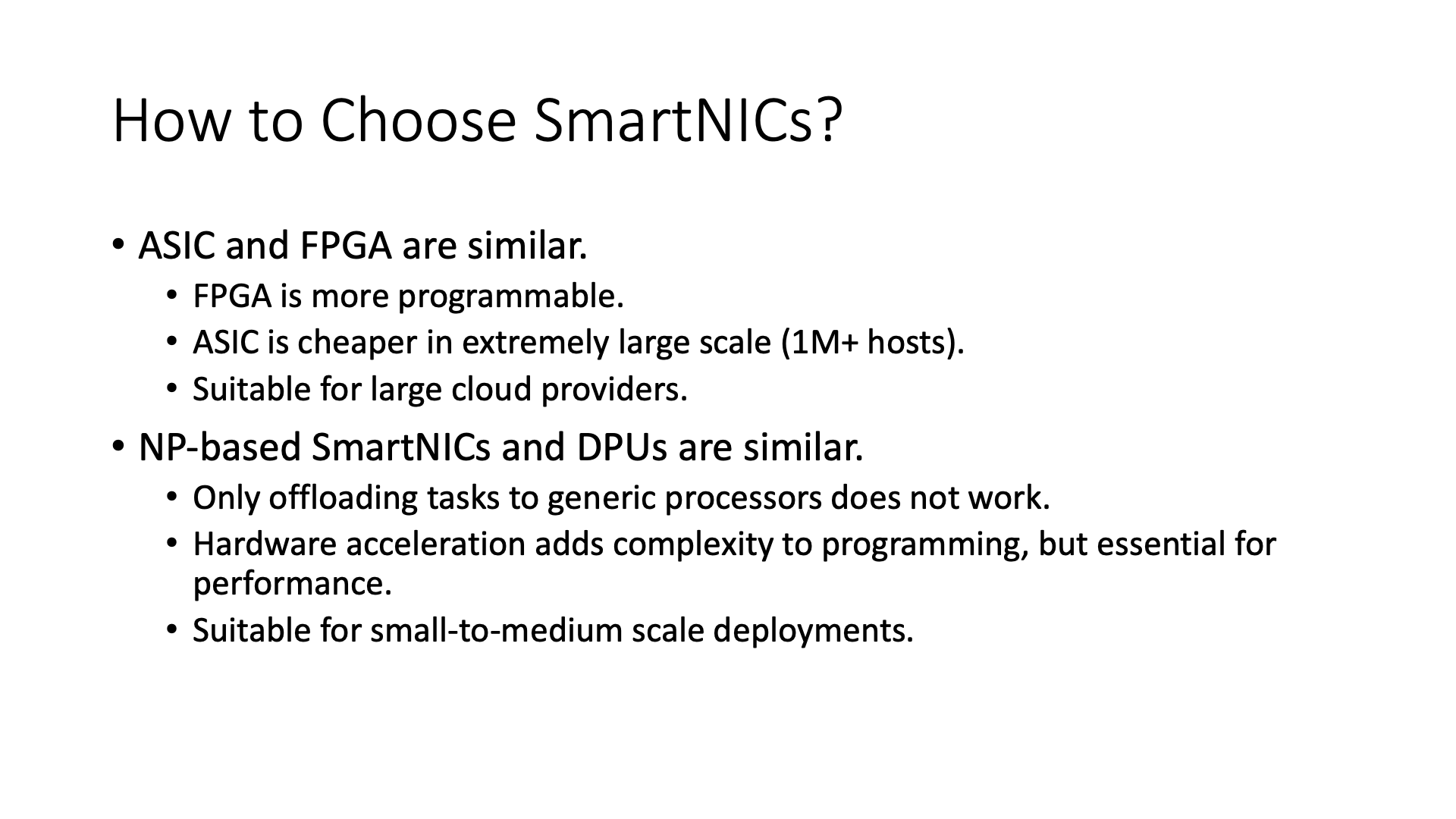
So how to choose these smart network cards?
In fact, the main difference between them is that ASIC and FPGA are similar, and NP and DPU are similar. Generally speaking, if the deployment scale is particularly large, ASIC and FPGA may be more suitable.
But if it is NP and DPU, this is suitable for small scale, because in this way its development cost is much lower than ASIC.
There is also a problem here, which is a trade-off between hardware acceleration and its programmability.
Next, let’s briefly talk about Programmable Switches. Switches are another type of programmable network device, besides SmartNICs.
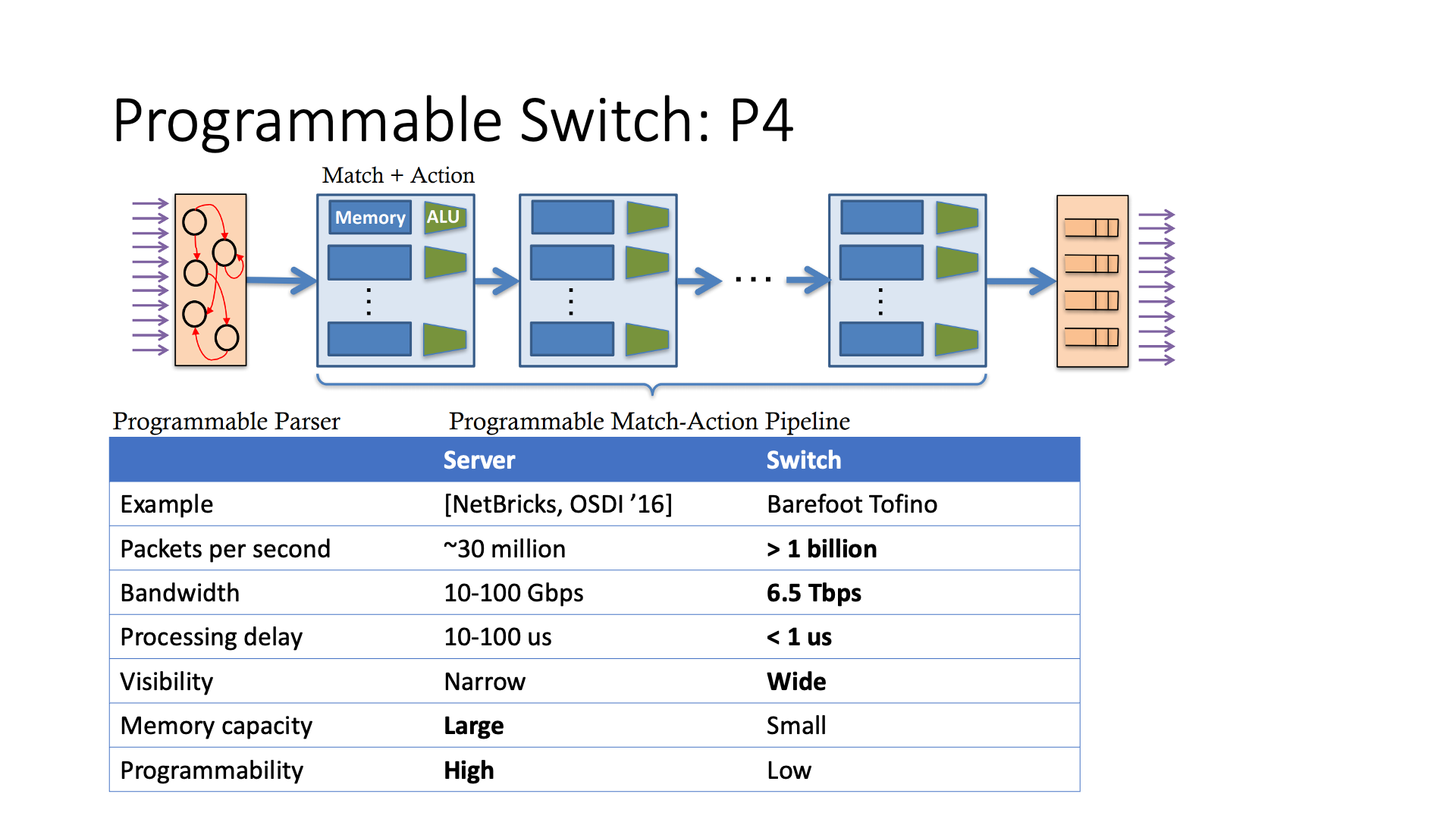
Currently, the hottest programming abstraction for programmable switches is P4. Now, about 1/3 of SIGCOMM papers have some relationship with P4.
Earlier, we mentioned that programmable NICs often have match action tables, whether it’s the GFT in Microsoft’s FPGA, the lookup table in NP, or the hardware-accelerated lookup table in DPU. The most basic abstraction in P4 programmable switches is also the lookup table. The lookup table matches some fields on the packet header and then performs the specified operation.
In fact, traditional switches also have lookup tables. What’s the difference with P4? The functions in the lookup table of a P4 switch are more abundant, such as simple calculations and state storage. In addition, the depth of P4’s lookup table is relatively deep, generally 16 levels, while the general lookup table in traditional switches does not exceed 3 levels. This way, P4 switches can complete more complex logic in a pipeline manner.
With programmable switches, what can we do? Let’s give a few examples.
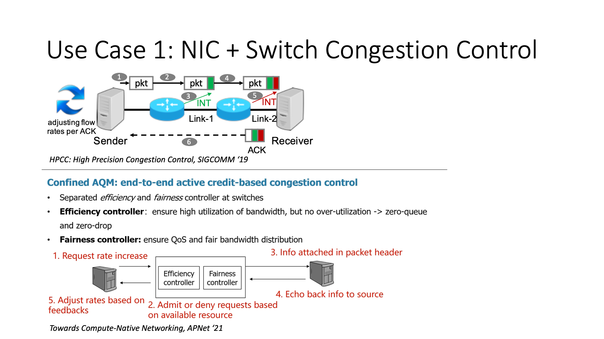
First, it can do congestion control in coordination with a smart network card and network switch. This is probably the most suitable and reliable thing for a programmable switch to do.
For example, how does Alibaba’s HPCC (High Precision Congestion Control) work? Traditional congestion control, if congestion is encountered on the switch, waits for the congestion signal to be sent to the other end, then returns, and then slows down at this time. But this brings a problem, that is, the slowdown may not be particularly accurate. So the HP in its HPCC is high precision, which means that it can have a very high accuracy on the switch, and then judge what the degree of its congestion is. This is the ability of the programmable switch’s INT (In-band Network Telemetry), and then it feeds back the degree of congestion more accurately, so it adjusts the bandwidth more accurately when adjusting the bandwidth.
Another work is by Huawei, which was mentioned in Tan Bo’s speech at the APNet 2021 conference. He proposed something called Confined AQM (Active Queue Management). Our main work is to implement a congestion control mechanism that cooperates with the end network. It is a hybrid control strategy of reactive and proactive, which is its main difference from traditional congestion control methods. In traditional network traffic control strategies, including HPC (High Performance Computing), it is usually to slow down after the network is congested.
However, our goal is to control the network when it is not blocked, in the hope that the network will never be blocked. How to achieve the goal of never blocking? The way to achieve it is to request bandwidth allocation to the switch before sending data. This means that it is an allocation-based method. That is to say, if I want to send data, I will not send data immediately, but first request bandwidth allocation to the switch. Then, after the switch has allocated credit, I send data according to the amount of credit allowed. In this way, I can ensure that the amount of data sent in any RTT will not cause queue accumulation. In this way, we can achieve almost zero queue access, which is a new method.
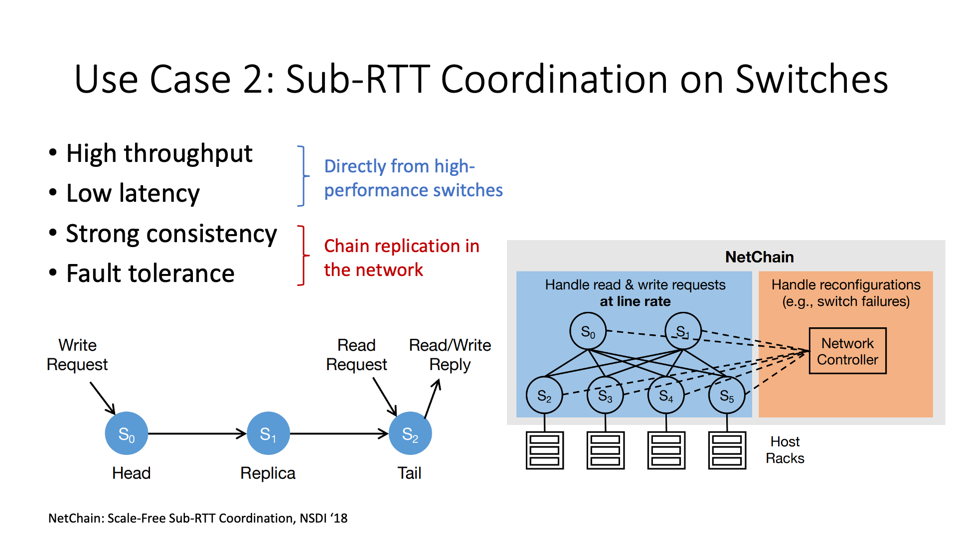
The second use of programmable switches is to accelerate distributed systems, which is the most published academic research.
Distributed systems often need to do some coordination work, such as the work of issuers. The issuer is to number each message, and then the distributed system needs to use these numbers when dealing with consistency. Originally, the switch did not have this function. It needed to be sent to a centralized host, let it number all the messages, and then sent to the target host. This issuer host may become a bottleneck. Now, the switch has this function, and the message is automatically numbered when it flows through the switch. In this way, all the messages on the network are naturally numbered, and I don’t need to go back to the host, which will be more efficient.
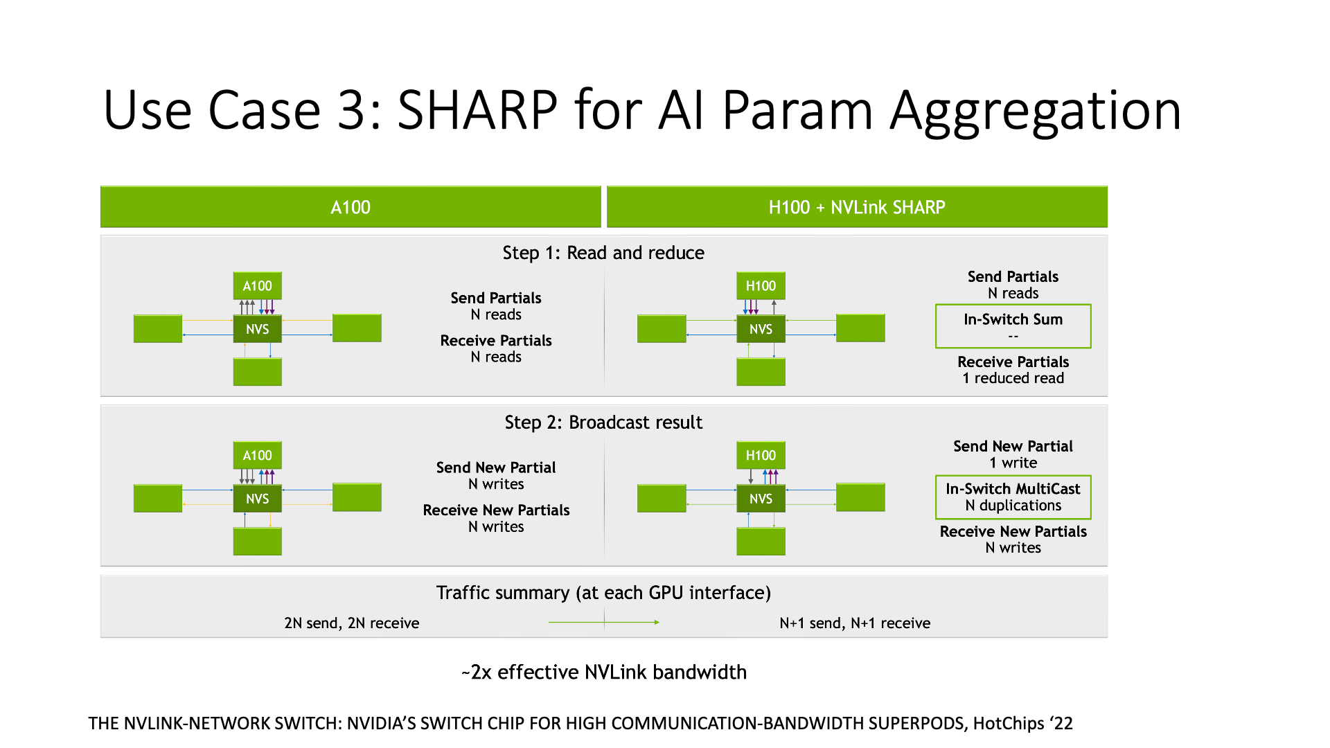
The third type of research is related to AI, such as Nvidia’s SHARP, which is for data aggregation. In AI training, some data aggregation processing is usually required, such as calculating the average gradient of each node. If using traditional methods, I need to collect the gradient values of each node, and then calculate the average value on the host. But now, the switch can directly calculate the average value, and the number of data transmissions has been reduced from the original 2n times to n times, saving half of the bandwidth. What’s the benefit of saving bandwidth? In large-scale training, bandwidth is actually quite scarce. When bandwidth becomes a bottleneck, SHARP can improve performance.
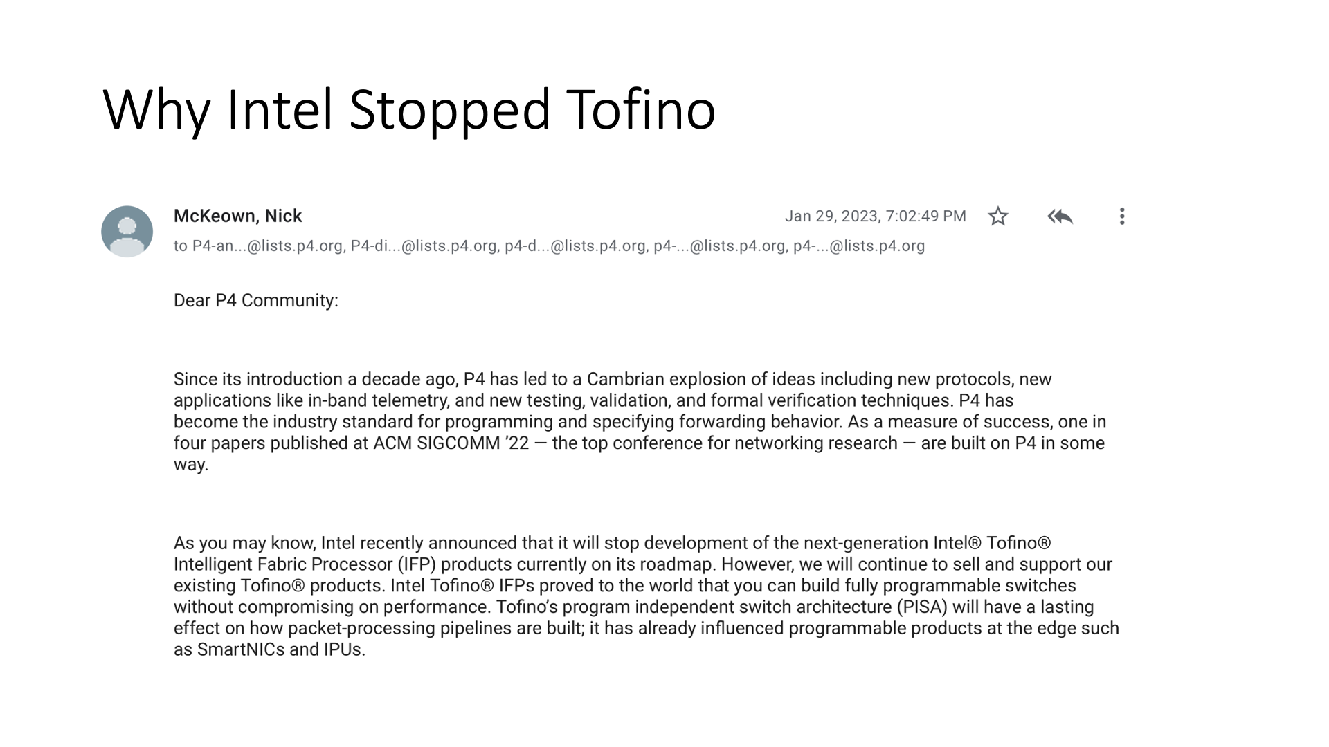
The AI-related SHARP mentioned earlier is a function of Nvidia switches. The INT required for the first type of congestion control is a function of many switches, including Broadcom switch chips. But the second type of work, accelerating distributed systems, requires Barefoot’s Tofino switch. Unfortunately, after Intel acquired Barefoot, this type of switch has been discontinued.
We speculate that the main reason Intel discontinued this type of switch is probably because they want to focus primarily on CPUs and IPUs, which are similar to DPUs. This is because Intel’s main product is the CPU. If a switch can do the job of a CPU, then the CPU might not sell. This is Intel’s strategic choice to put all functions on the host, not on the smart switch.
Including the PCIe controlled by Intel, it is also a slow squeeze of toothpaste, which is also a business choice, hoping that peripherals will always be supporting roles, and the core computing stays on the CPU, with the CPU always being the boss within the system architecture.
However, I believe that other manufacturers, such as Broadcom, Huawei, and Nvidia, their switches all have many smart features, and will continue to develop in this direction in the future.
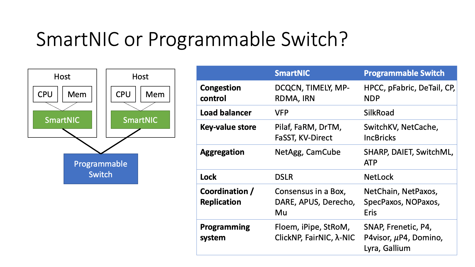
In switches and smart network cards, there is actually a lot of research work, including some work in academia. Some work is done on the switch, some is done on the smart network card, including many different researches, such as data aggregation, traffic control, etc.
But there is a choice problem here, because the field of view of the smart network card (SmartNIC) is relatively narrow, it can only see its own data. But its computing power is relatively strong, because it does not need to handle a large amount of bandwidth, so it only needs to process its own data, so its computing power will be stronger.
On the other hand, it can better integrate with some protocols, such as the RDMA protocol. And the switch can see more data, so functions like traffic control must be implemented on the switch, otherwise it doesn’t even know if there is a blockage on the switch.
There are also some functions, such as data aggregation and coordinators, etc., which are obviously more suitable for implementation on the switch. So in different scenarios, each device has more suitable functions.
Earlier we saw that various network devices are becoming smarter and smarter, including switches and network cards. Another way is to put all the smart functions on the end side, instead of implementing them in the switch and network.
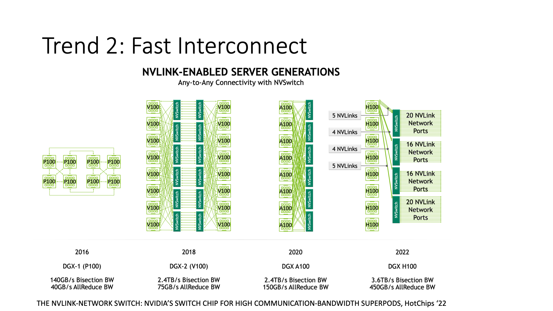
For example, most of Nvidia’s network cards have adopted this method, because we see Nvidia’s GPU, its initial architecture is to use NVLink to directly connect these cards. Why connect directly instead of using PCIe? Because PCIe is too slow. The development of PCIe is like squeezing toothpaste. Why? Intel always wants to put everything on the CPU to do, he is not willing to increase the middle bandwidth too much, because once the middle bandwidth is increased too much, such as GPU and storage devices can directly access, bypassing the CPU, then no one will buy high-end CPUs, right?
So, he is considering from a business perspective, he is not willing to increase the PCIe bandwidth too much. Nvidia saw this, and he found that the bandwidth between GPUs has become a bottleneck, what can he do?
Nvidia did two things. First, he went to make an NVLink network, we can see that the bandwidth of NVLink is getting higher and higher, even the NVLink switch has been made, originally it was just communication inside a machine, now it can communicate within a cluster.
Second, it cooperates with ARM to achieve a high-performance CPU, such as their new Grace CPU, which is also directly high-speed interconnection with the GPU. There is no PCIe thing in the entire Grace Hopper architecture, and there is no Intel thing.
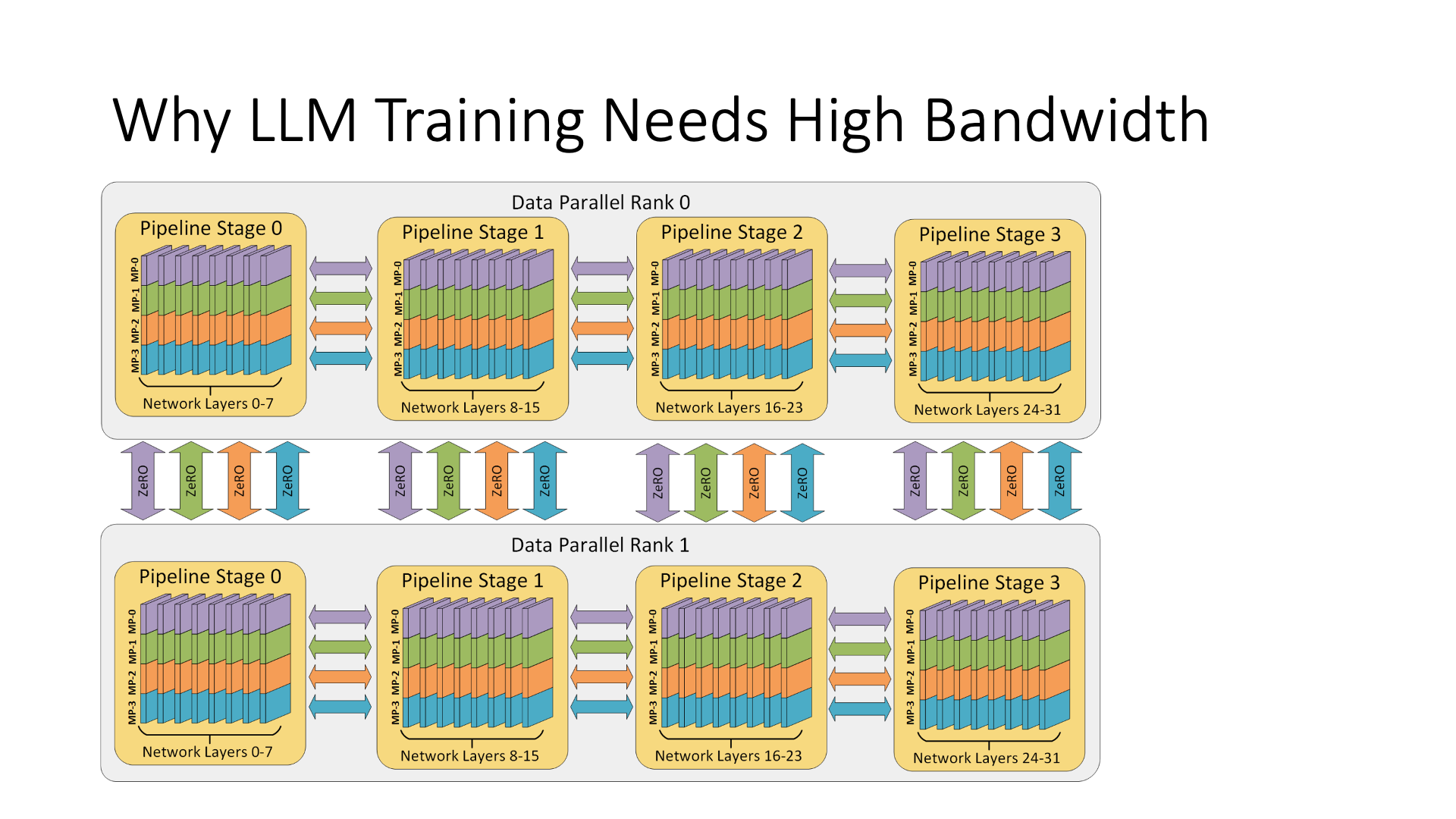
So, there is a question, why does AI need a very high bandwidth?
Because I need to do model parallelism. In model parallelism, I can assign different parts of the model to different cards, for example, I have 64 cards, each card is responsible for calculating a part of the model, and then they communicate with each other. The simplest idea might be that since the model has many layers, can I just divide it into many layers? This is called pipeline parallelism.
The first is that a GPU may not be able to hold all the data required in the training process of one layer. The second problem is that even if one layer can be put down, if there are too many layers divided, and the pipeline is too deep, the performance will actually decline. Therefore, we need to use tensor parallelism and pipeline parallelism at the same time in model parallelism, in addition to model parallelism, there is also data parallelism, these three parallel methods need to be used together.
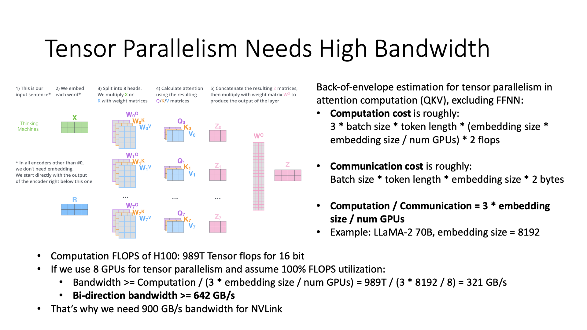
So, why does tensor parallelism require a lot of bandwidth, we can do a simple estimate.
For example, only calculate the computation cost of the attention QKV part, ignore the FFNN part. We first calculate the computation cost, that is, the required FLOPs, and then calculate the communication cost. Then the ratio of computation to communication is 3 times the embedding size divided by the number of GPUs doing tensor parallelism, right?
Then, if I want to train a LLaMA 70B model, after substituting the calculation, the result is about, if I have 8 graphics cards and want to do tensor parallelism, I might need a 642 GB/s bandwidth.
So we know why I need 900G bandwidth in NVLink, 128G PCIe bandwidth is not enough. The domestic castrated version of 400G bandwidth may not be enough.
Although this is a rough calculation, it is approximately of this order of magnitude.
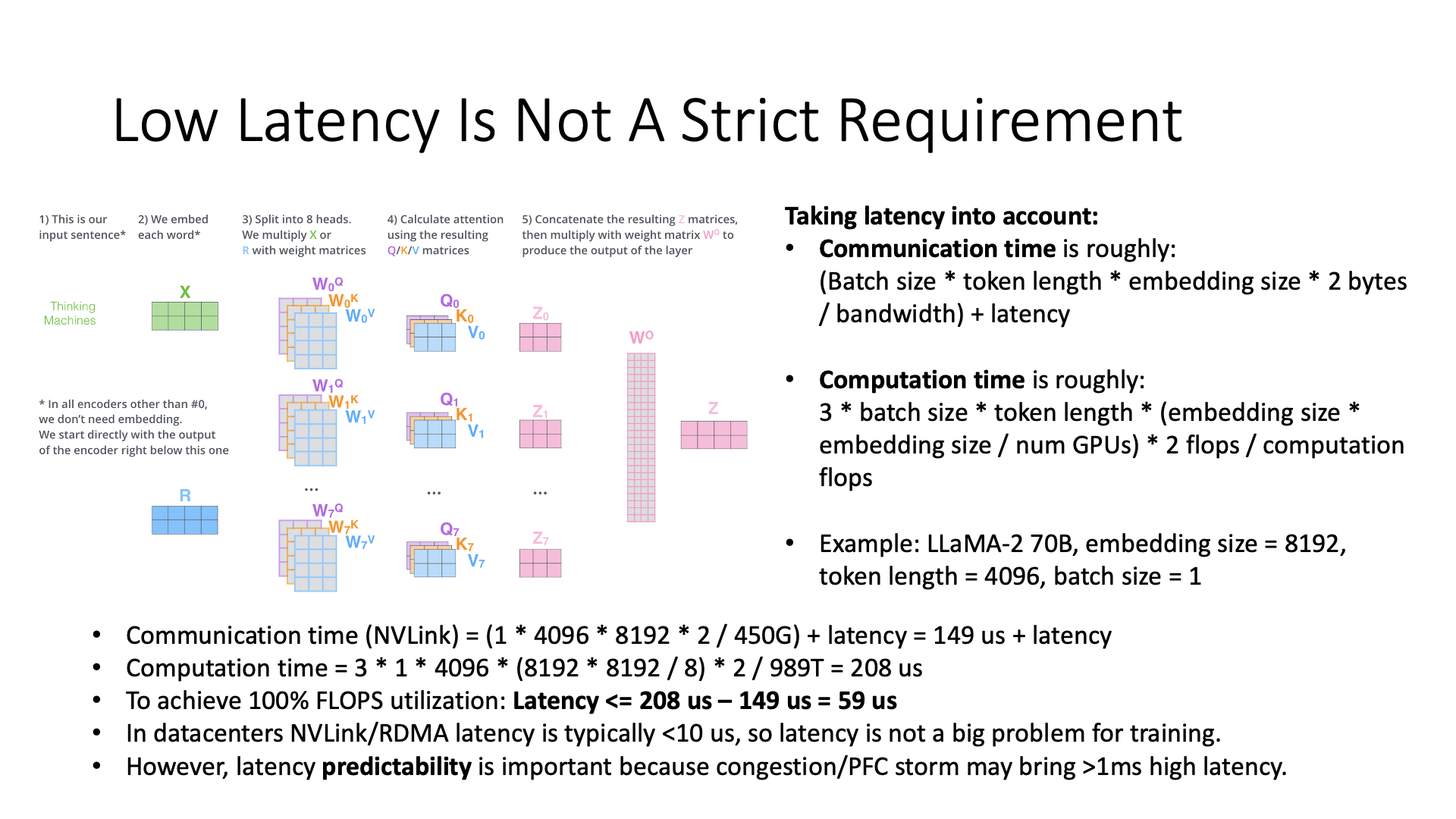
Although tensor parallelism requires high throughput, the latency requirements are not as high as imagined, because the tensors transmitted during the AI training process are relatively large.
In terms of latency, let’s simply calculate the total communication time and computation time, add the latency, and then we can see that if tensor parallelism is performed, because the transmitted data is small, we can see that only 16MB of data is transmitted at a time. Some people say that 16MB of data is already not small, right?
But if you divide it by its total bandwidth, you will find that this 16MB data is transmitted in 149 microseconds. This calculation only needs 208 microseconds. So if you want to fully utilize the computing power on the same 900G network, of course, fully utilizing the computing power is an ideal situation. If you can fully utilize it, then its latency needs to be below 59 microseconds.
So it needs to design something like NVLink to achieve direct communication between GPUs. If I go around from the CPU, the latency can’t stand it, and the bandwidth will also be discounted, because the bandwidth of the CPU is definitely not as high as the bandwidth of NVLink. This is the demand for AI training.
However, 59 microseconds is not a high requirement. For example, the end-to-end delay of NVLink is less than 1 microsecond, and the delay of the RoCE RDMA network is also less than 10 microseconds. As long as you don’t consume too much delay on the software protocol stack, it is acceptable. But one thing to be careful about is tail latency, such as network congestion, or a PFC Storm occurs, then the network latency may suddenly rise to 1 millisecond or even higher, which is unbearable. Therefore, the predictability of network latency is very critical.
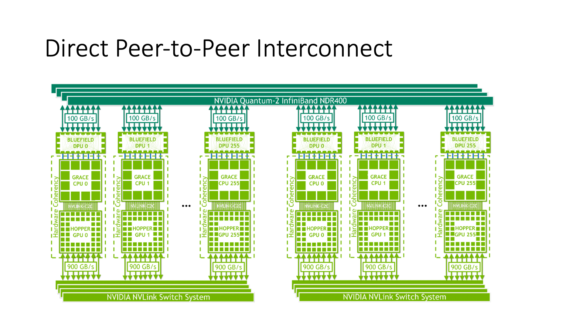
So, NVIDIA designed an interconnect architecture called Direct P2P, which is the Grace Hopper architecture. In this architecture, all GPUs are interconnected through NVLink.
Then, the CPU part, through the Bluefield DPU and the network, connects it, which is its overall structure.
The CPU part above is actually used for large-scale communication, and the GPU part below is used for small-scale communication. The CPU part above is more used for cloud-related communication.
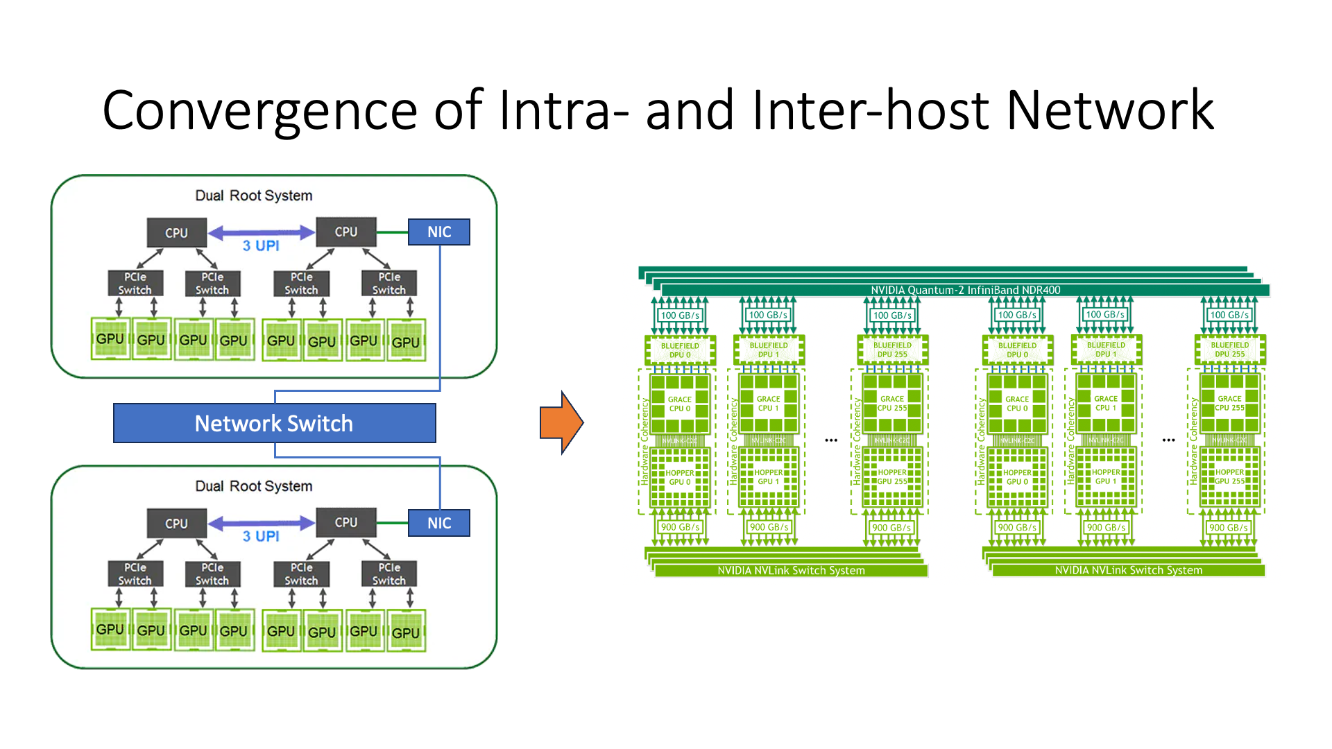
At this time, we can see a major difference between the old architecture and the new architecture, that is, in the old architecture, all GPUs are hung on the CPU through PCIe, and then the CPU connects to the network card and then communicates. So at this time we can see that the communication performance between GPU and GPU is actually poor, right? The latency is also high, and the bandwidth is also low. But if in the new architecture, the communication efficiency between GPU and GPU will be much higher.
This reflects a point, that is, the bus inside the host and the network between the hosts are integrated. In this picture, you can’t tell which machine, where is inside the host, and where is between the hosts, right? The previous architecture, we draw a box and a machine, right? Then the original architecture clearly distinguished the communication inside and outside the host, and the communication efficiency between the hosts will be lower, right?
This is a new change, including the new type of switching network that Huawei is doing. It is actually a structure similar to NVLink, which allows the communication inside and outside the host to be integrated.
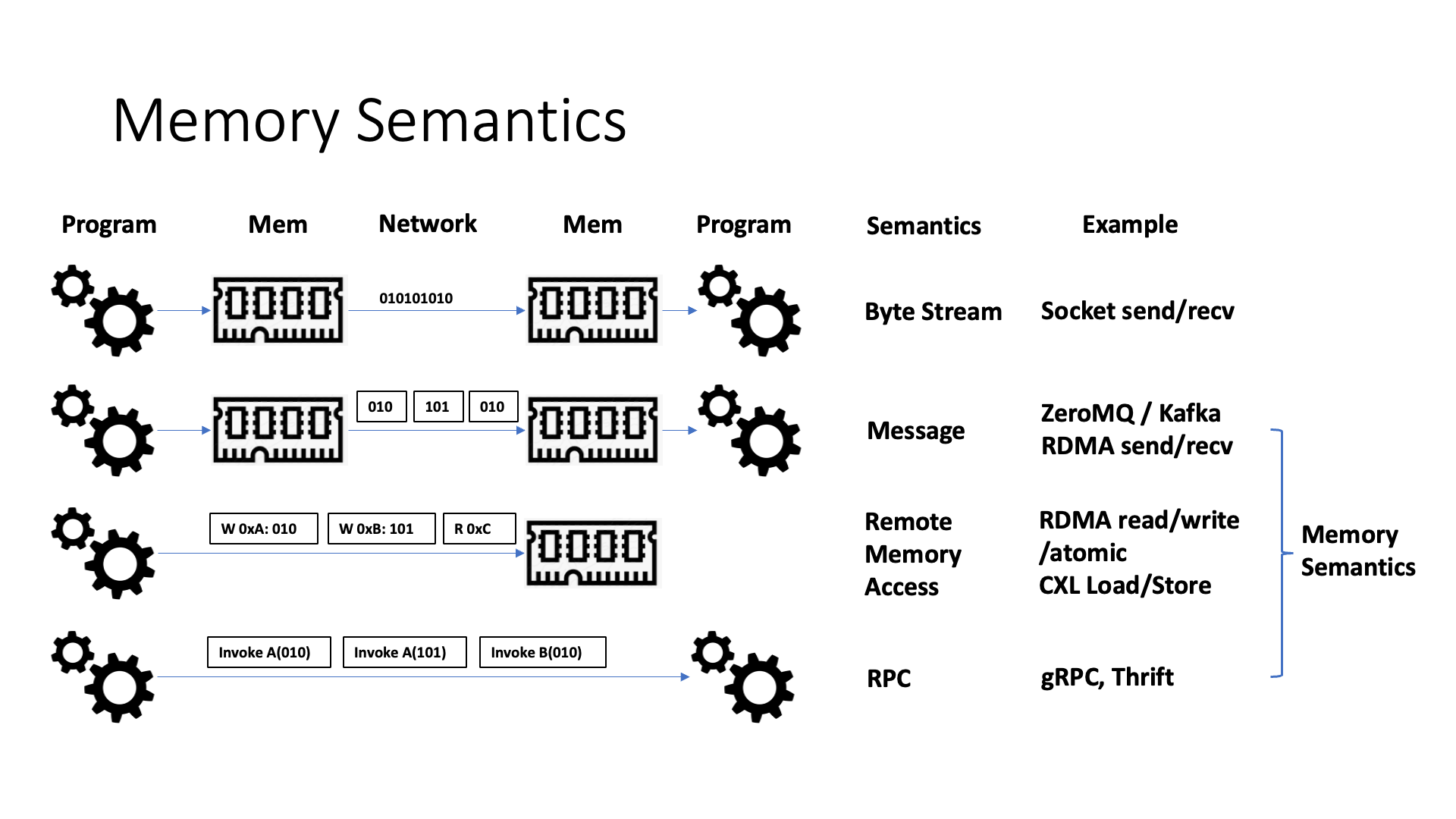
Like the NVLink interconnect protocol, the communication is actually using memory semantics. Memory semantics are different from the original byte stream semantics. The byte stream is the simplest sending, such as socket, but the efficiency of the socket is relatively low. Why is the efficiency low? First of all, the byte stream of the socket is strictly ordered, so if I want to send a bunch of things at the same time, I can’t fully utilize parallelism.
The second is because there is no message boundary semantics in this byte stream, so there often needs to be a packet splitting thing inside. For example, the application layer protocol, whether it is the HTTP protocol or other protocols, there is actually a concept of an application layer message header inside, and the application layer needs to extract the message from the byte stream, at this time its efficiency will be lower.
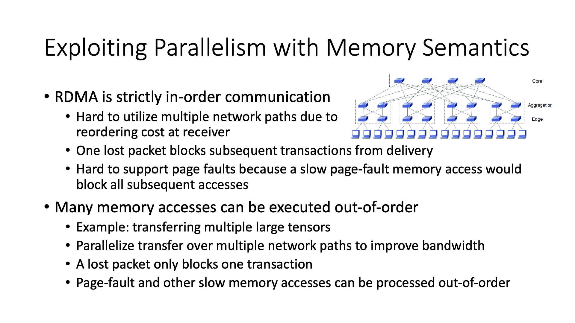
Then after we use memory semantics, it solves the problem of strict ordering. Whether it is RDMA or traditional byte stream, it must be an in order strictly ordered way of communication.
With memory semantics, we know that memory access is not strictly ordered, so it can fully utilize the multiple paths between various nodes, because there are many paths to go between multiple machines in our data center network.
What other benefits are there, that is, the efficiency of fault recovery is also relatively high, for example, if I lose a packet here, and then if you are sequential transmission, all the transactions (memory access transactions) behind are waiting behind, but if it is a disorderly transmission mode, this lost packet can only block the transaction it is in, and other transactions can be executed concurrently.
The last point is that RDMA does not currently support page faults, meaning that memory is always first-class, but the disk is second-class. Therefore, in the world of RDMA, it cannot directly access the contents of the disk. Why does reading from the disk require a page fault? Because it needs to fetch the contents of the page from the disk into the memory in the operating system, and then RDMA can access it.
RDMA does not support page faults mainly for two reasons. One is that the current network card may not be able to cooperate well with the memory management of the operating system; the second is that in the sequential transmission of RDMA, page fault is a heavy process. If you read 4 KB of content from the disk without any cache, it will take at least tens of microseconds, which will block subsequent requests and reduce efficiency.
If we introduce a disorderly transmission mechanism, then the page fault handling on the network card can be improved, which means that the address can actually be completely virtual, partly in the host’s memory, and partly on the disk. The remote application accessing the data does not need to care whether the data is in the host memory or on the disk. If it is on the disk, the network card can fetch the data from the disk, check the page table, and after checking, it can be fetched from the disk. In this way, the overall access efficiency may be greatly improved, and the network card can be used to help handle the page fault work.
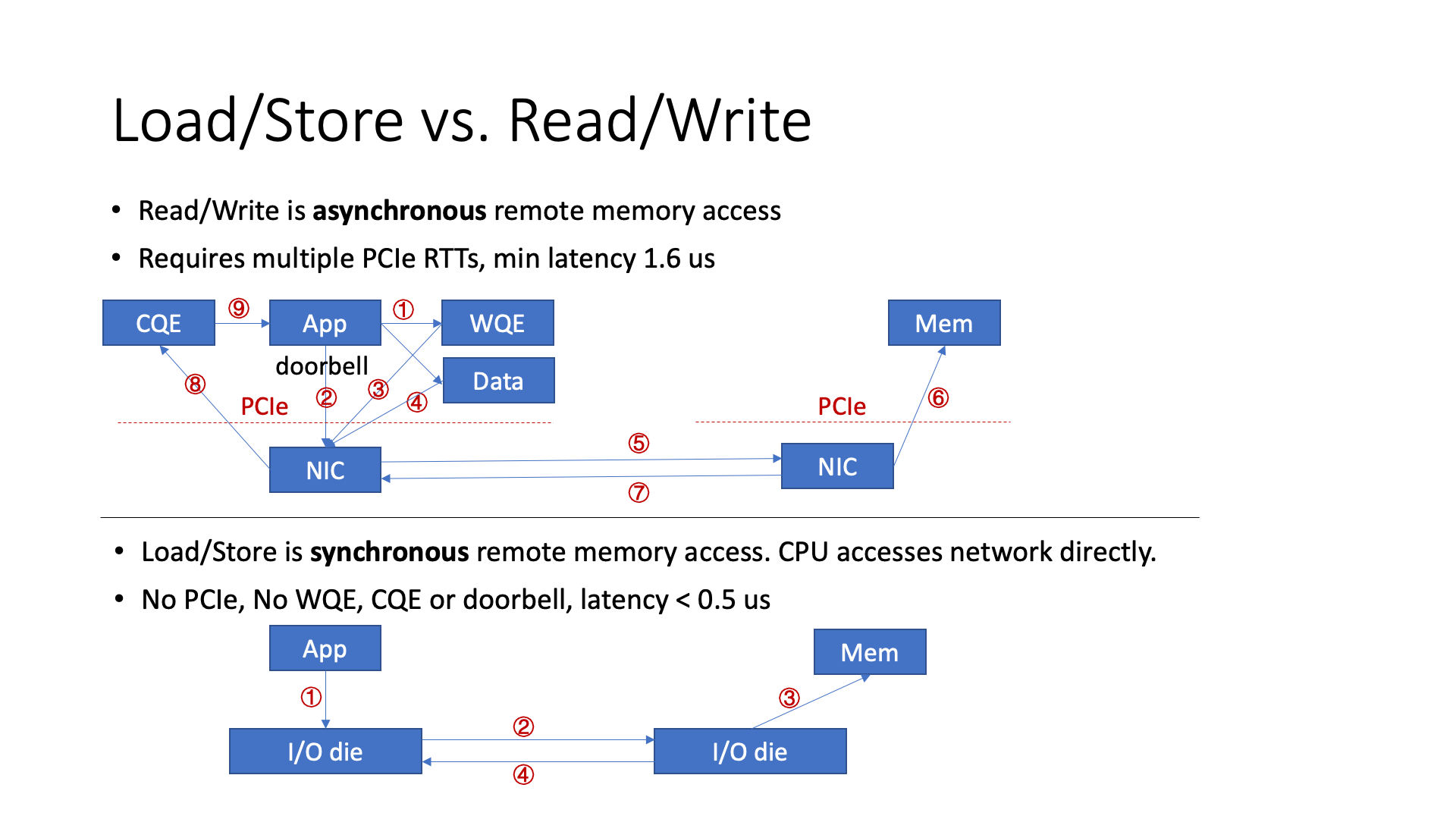
Another possible improvement is to use load store to replace read write. Read write is an operation in traditional RDMA, and the process of transmitting data is actually very complicated, and the whole process is very long. If we use load store, then it is actually a synchronous method, the whole process is shorter, so the latency will be shorter.
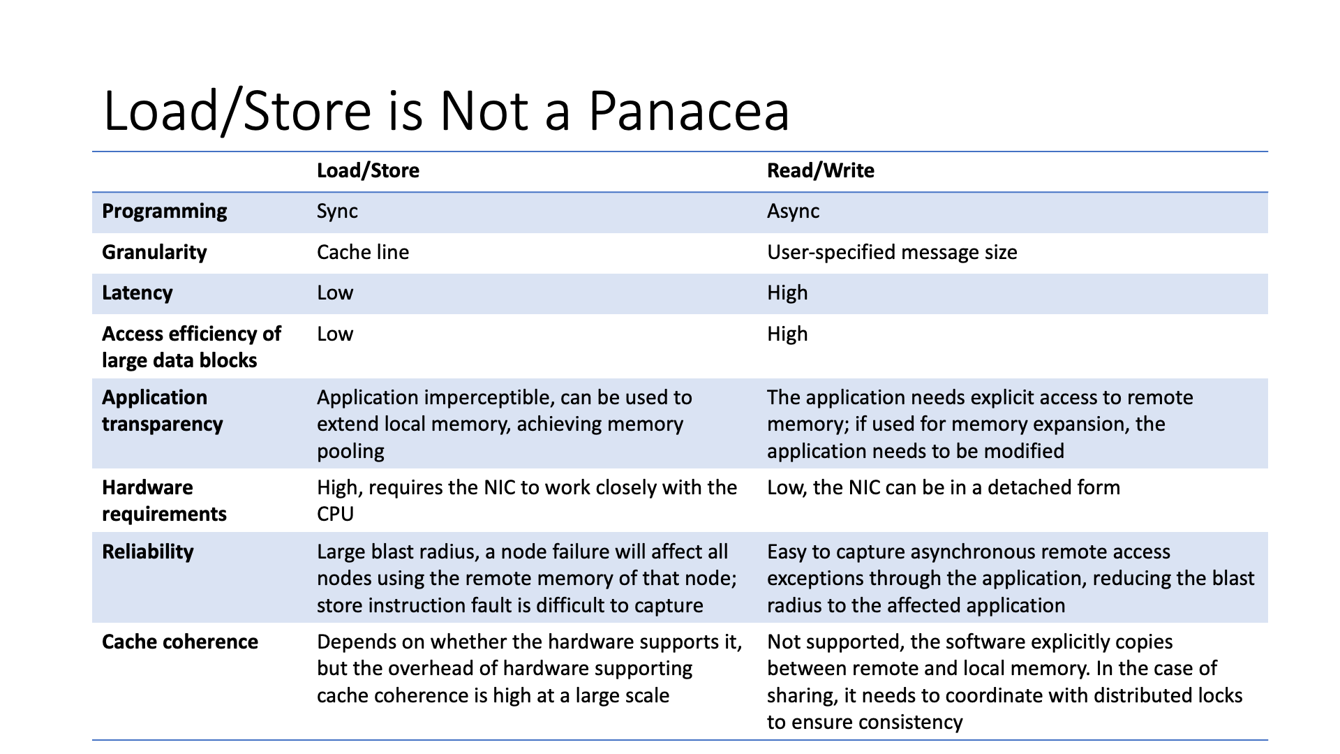
But this is not applicable to all situations. Although load store programming is simple, if it is a large block of data, each core needs to wait, its pipeline depth is limited, and the efficiency may be lower.
In addition, load store’s support for faults is also insufficient. If a memory access is stuck, the CPU may crash directly. Even if the load request can easily locate which process it is, the exception caused by the asynchronous store instruction is difficult to handle, and the CPU itself cannot remember which process caused the store exception. But if you use the asynchronous method of read write, fault handling will be much easier.
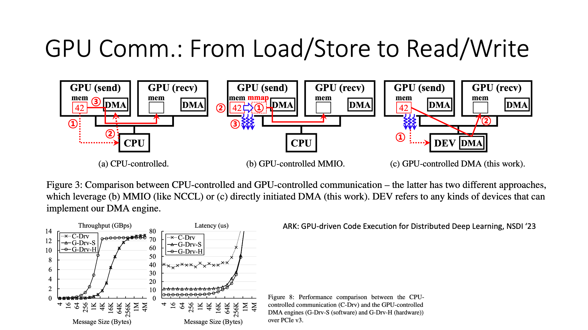
Recently, Microsoft has also done a job, they have changed load store to read write, making the communication between GPU and GPU more efficient than the original load store. That is to say, under the same hardware conditions, if I use the method of read write for communication, when the data volume is large, it may be more efficient than the original method of directly accessing remote memory through CPU or GPU load store instructions, which can reduce some CPU and GPU core waste, and also reduce cache waste.
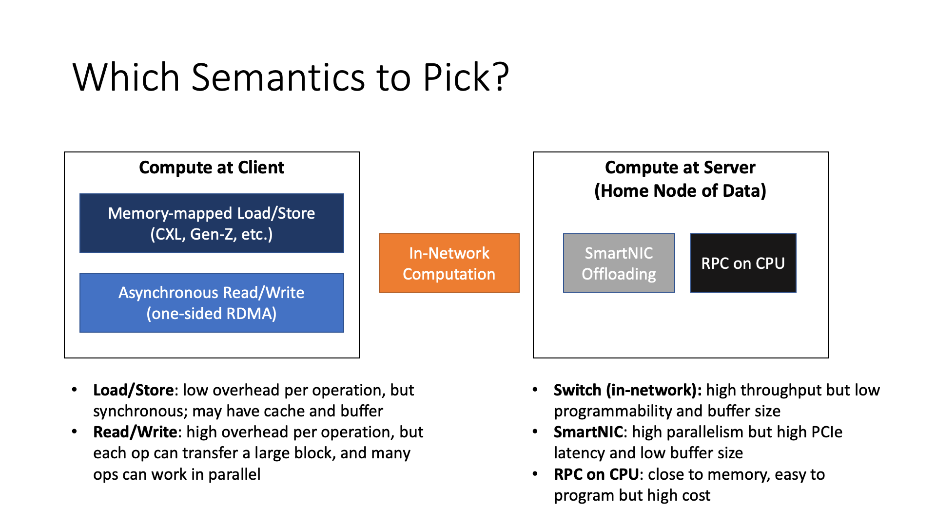
Earlier we discussed the semantics of direct memory access, including load store and read write, each with different advantages and disadvantages. Even earlier, we discussed various smart devices in the network, including smart network cards and programmable switches.
Assuming the data is remote, then we have several different data access methods. The simplest is to put all the calculations on the local CPU or GPU, that is, to use memory semantics to directly access remote memory, without relying on network devices, then there are different ways such as load store read write.
And if you put the calculation in the network, including using SmartNIC offloading, and In-Network Computation and other different choices. Of course, if the data is remote, SmartNIC also needs to use load store or read write memory semantics to access remote data. If you use a programmable switch, because the programmable switch currently does not have the ability to directly access remote memory, you need to send a request first to fetch the data from the remote, and then use the programmable switch to process it on the way back.
I can also put the calculation on the remote CPU, for example, I can make an RPC call, that is, send the calculation task to the data nearby, which is also a choice.
Each choice has different trade-offs, so it is not a one size fit all solution. In the future, there is an interesting job, whether it is possible to make an automated system that can decide where to put the calculation.
Finally, I believe that AI and Cloud (cloud computing) will definitely be integrated in the future.
Traditionally, AI clusters and cloud computing clusters are separate. This means that the network bandwidth (Bisection Bandwidth) transmitted between the AI cluster and the cloud computing cluster is lower. Traditional AI processing and big data processing are relatively separate processes, so they do not need so much network bandwidth. But in the future, AI will definitely be an indispensable component in the process of big data processing, and there will be a lot of data interaction in the middle. The communication efficiency of the separate cluster is relatively low.
Furthermore, GPUs within an AI cluster usually communicate directly with each other, without the need for virtualization. Even if a smart NIC is added for virtualization, the overhead is too high. Therefore, many people believe that AI networks and cloud networks cannot be integrated. But why must virtualization be on the CPU or smart NIC? Why can’t high-speed communication hardware natively support virtualization? Just because NVLink doesn’t support it now, doesn’t mean it’s impossible.
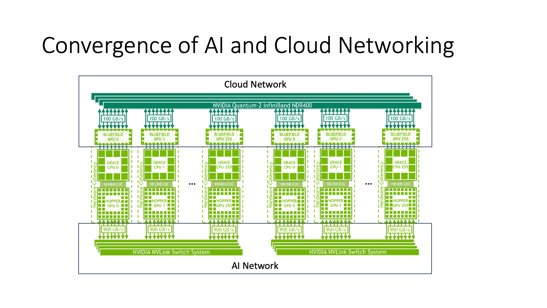
In NVIDIA’s model, the AI network is the box below, and the Cloud network is the box above. That is, each computing unit can be considered as a GPU plus an ARM CPU, with the Cloud network connected on the CPU side and the AI network connected on the GPU side. The CPU and GPU are also interconnected through a high-speed network.
Can you clearly distinguish which is inside the host and which is between hosts? This is the integration of intra-host and inter-host networks, and the concept of the host is diluted in network interconnection. When each computing unit needs to perform operations related to the Cloud, it can access the Cloud network through the DPU (Data Processing Unit), which can solve the problems related to virtualization that we mentioned earlier.
The efficiency of direct interconnection between GPUs is the highest. Because its communication bandwidth is an order of magnitude lower than the Cloud network above, it is 10 times worse. Therefore, we can add a DPU in the Cloud network above, but it is best not to add a DPU in the AI network below, otherwise the efficiency will be very low.
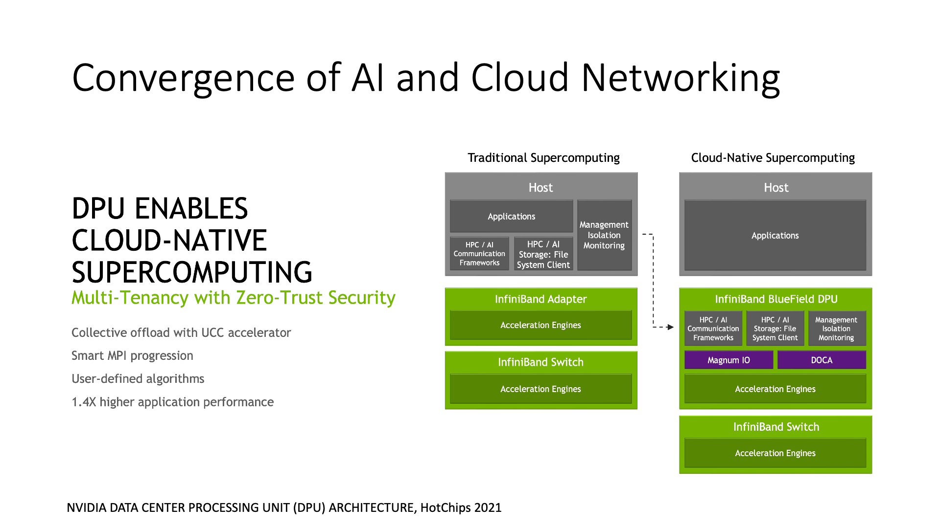
In the DPU, a lot of acceleration work can also be done, and some network functions on the host can be moved to the DPU. The focus of this picture is the acceleration of AI-related collective communication. Collective communication is not as simple as just passing data, there is also a calculation process, which is to summarize (reduce) the data uploaded from different nodes. Whether it is sending and receiving network messages or calculating reduce operations, it consumes a lot of CPU resources. Therefore, the smart NIC, that is, the DPU, can do the offloading of collective communication.
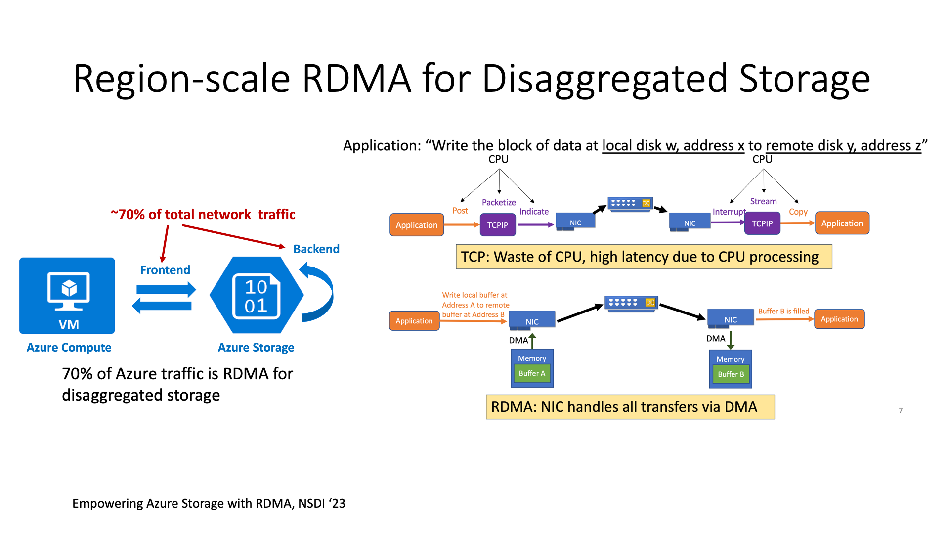
In terms of Cloud networks, RDMA is a very good technology. Next, we will introduce the largest RDMA deployment in the world, which is Microsoft Azure’s full network deployment of RDMA, mainly used to accelerate cloud storage.
What’s special about Microsoft’s RDMA deployment? Previous RDMA deployments were all within a cluster, at most at the level of a data center. But Microsoft’s RDMA deployment is the entire region, and all communication across data centers in a region also uses RDMA.
The RDMA here is not Infiniband, but RoCE (RDMA over Converged Ethernet). IB cannot cross data centers.
In the entire network of Microsoft Azure, more than 70% of the network traffic is actually access to storage, which is very easy to understand. Because storage is all disaggregated, in a dedicated storage cluster. All accesses to block storage, NAS disks, and object storage have to go through it, so the communication bandwidth generated by the storage system is even higher than the communication bandwidth directly generated between hosts.
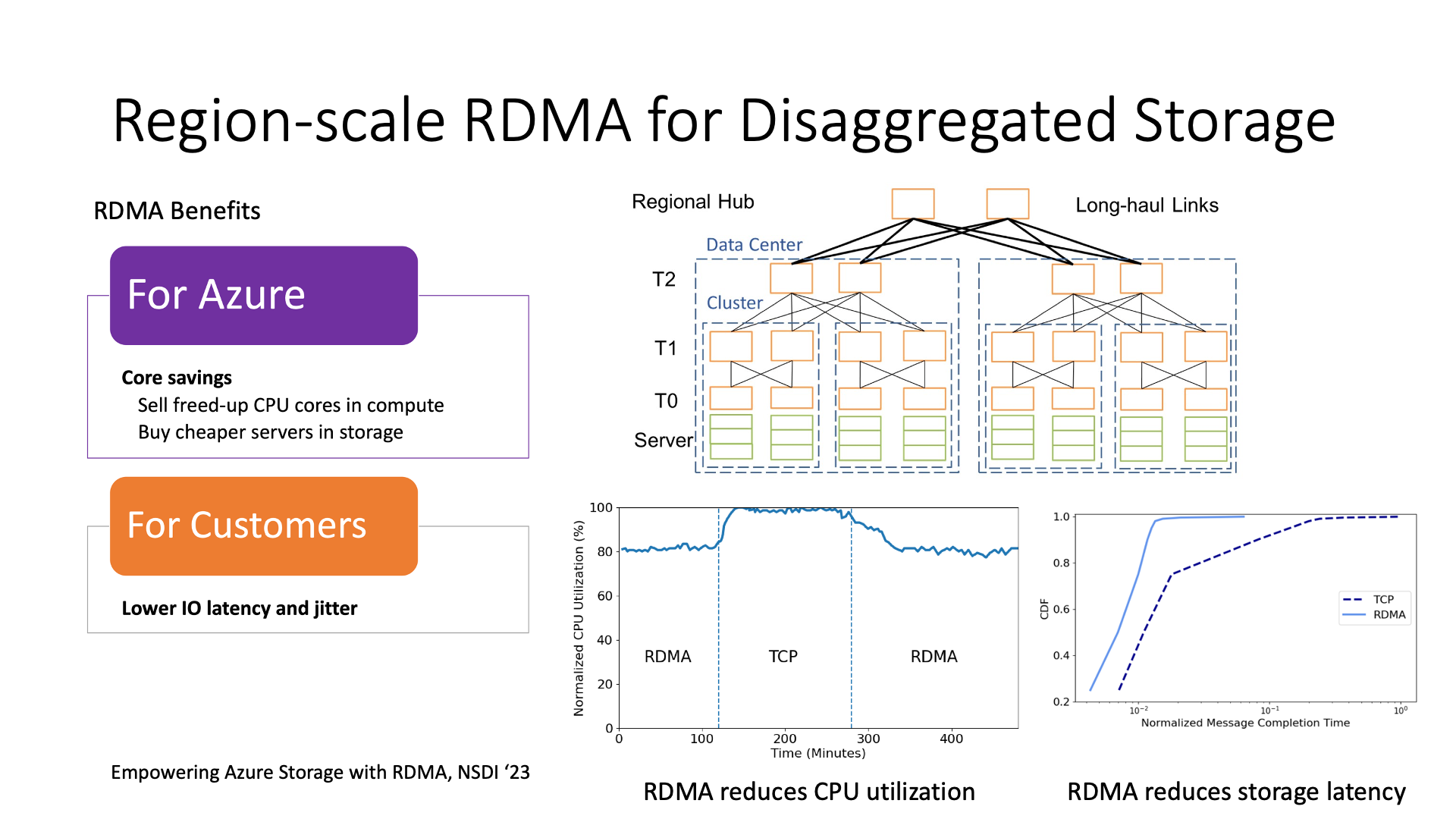
Using RDMA instead of TCP can reduce a lot of CPU waste on computing nodes. For example, in this picture, it shows that the CPU usage rate using RDMA is 20% lower than using TCP. Storage nodes can also reduce costs, because if all storage nodes use TCP, it means that they need a lot of CPU to process the network. If RDMA is used, it can save the CPU consumed by the network, and then cheaper CPUs can be used for storage nodes.
Another is a decrease in latency, especially a decrease in latency jitter, that is, tail latency can be significantly reduced compared to TCP, which is key to improving the QoS of the storage system.
The main challenge in deploying RDMA at the region level is actually the cross-data center switches at the top of the topology diagram. If you want to use RoCE in a small cluster of dozens of machines, it’s not that difficult, it’s basically plug and play.
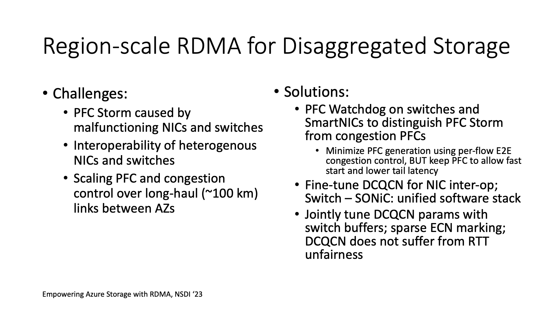
If RDMA has to cross data centers, and then has to go through these cross-data center distances above, about 100 kilometers, then this will bring a challenge. Because to eliminate congestion packet loss requires PFC (Priority-based Flow Control), it is hop-by-hop, that is, the buffer size of the previous hop must be large enough to accommodate a BDP (Bandwidth-Delay Product) message between these two hops, then a 100 Gbps connection of 100 kilometers requires a 1 millisecond RTT, which is a BDP of 12.5 MB. Each port needs so much buffer, the buffer of ordinary switches is easily not enough.
Therefore, Microsoft Azure bought some large queue switches, in fact, the buffer of the top-level switches is now very large, and then adjusted the buffer into shared queues, rather than each port fixed to occupy a certain memory queue.
They also did a lot of work related to network card and switch configuration. For example, many people are worried about the DCQCN congestion control algorithm. In fact, DCQCN, because it is rate-based rather than window-based, has a good feature that it does not cause high RTT connections and low RTT connections to be treated unfairly in competition. For example, on the Internet, if a cross-national connection and a local connection are in competition, the cross-national connection will definitely suffer. But in DCQCN, the connection across data centers and the connection inside the data center are fair. Of course, they also did some tuning on the parameters of DCQCN.
But the problem is bigger with PFC. When the scale becomes larger, for example, it is no longer a cluster of thousands of machines, but a cluster of 100,000 machines, which means that many network cards will fail, and many switches will fail. These faulty network devices may generate a lot of PFC messages, endlessly, blocking the entire network, which is called a PFC storm.
PFC is originally used for flow control, it can backpressure, let the previous hop not send too much data, so as to minimize packet loss. However, traditionally many researchers have proposed that since PFC has the problem of storms and deadlocks, then I will never use it in the future, I only rely on end-to-end congestion control. But in fact, end-to-end congestion control cannot completely solve all problems.
For example, in the case where we access the same node at many nodes at the same time, that is, the so-called incast situation, no matter what congestion control algorithm is used, it will eventually cause congestion. At this time, we still need to rely on hop-by-hop PFC to control network traffic to ensure that the network will not lose packets due to congestion.
Microsoft Azure’s solution is to keep PFC, but it can distinguish whether it is PFC caused by failure or PFC caused by congestion. The logic is actually very simple, because if it is caused by a failure, it will keep sending, if it is caused by congestion, it will block for a while, and it will not block later. Therefore, if you encounter PFC caused by failure, the switch and smart network card will filter out these PFCs and report a failure.
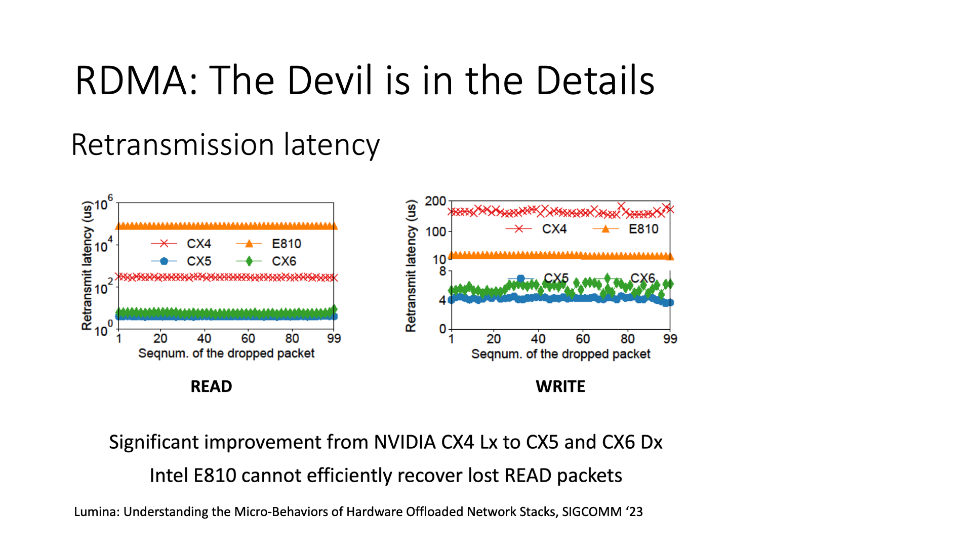
The process of deploying smart network cards may be complicated, because different network cards behave differently, and some network cards may perform poorly. For example, if you use a specific network card, such as the Intel network card in the picture, its packet loss recovery time may be very long. This kind of thing will not be written in the network card’s spec, and even a simple perftest test can’t find it, only in an environment with packet loss can this problem be detected. This is like choosing a GPU, not to say that the theoretical computing power looks high is definitely better, the devil is in the details.
To give another example, the interoperability between different network cards is a troublesome thing, because their implementation is different. For example, the old Mellanox network card only returns a CNP congestion notification message within one RTT when it encounters congestion, and the sender reduces the speed by half when it receives this message; but the new Mellanox network card returns a CNP notification for each congestion message, and the sender only reduces the speed by a small part when it receives this message. So if the old and new Mellanox network cards are put together for communication, when the old one encounters congestion when sending data to the new network card, then the new network card returns a lot of CNP messages, and the old network card suddenly reduces the speed to close to 0, this performance is definitely not good.
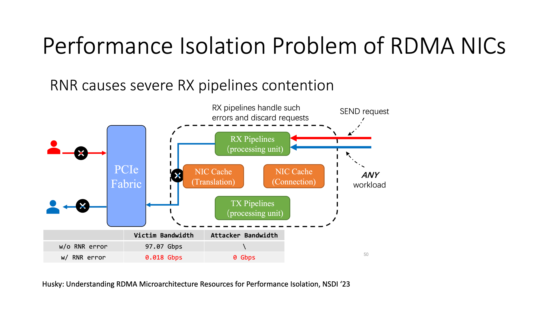
When using RDMA network cards, there will also be many security issues.
For example, DoS (Denial of Service) attacks, if a connection has many RNR (Receiver Not Ready) errors, that is, when the sent send request does not have a corresponding recv receive request, the network card will return an RNR message. But the network card handles this error message using the firmware inside the network card, and the firmware processing speed is slow, so once it starts to handle a large number of RNR messages, other operations will become very slow. This has broken the performance isolation of the RDMA network card.
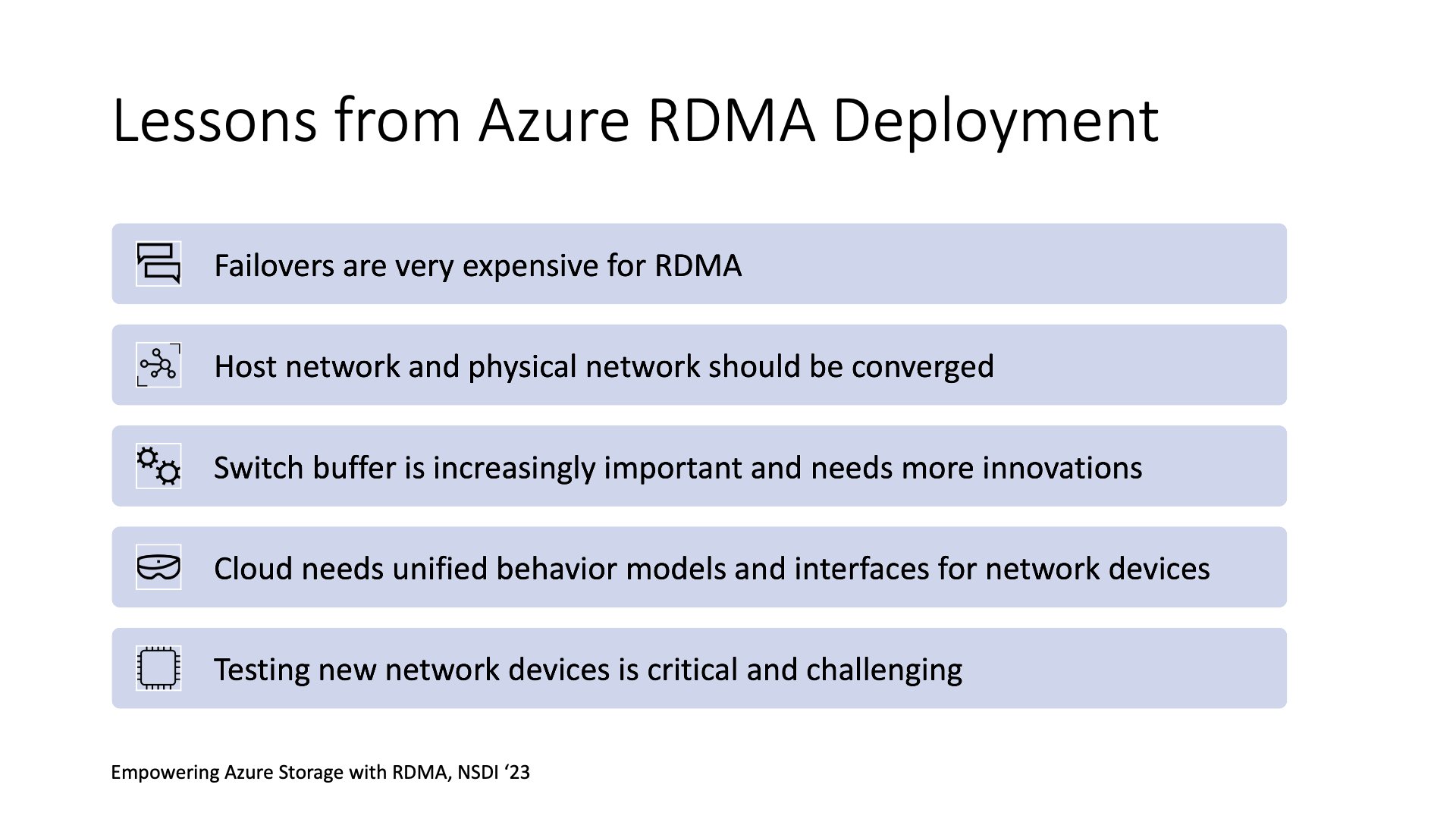
Microsoft also has many discoveries in the process of large-scale deployment of RDMA. First of all, fault handling is a bit troublesome. Secondly, the host and physical network need to work together, which is also a problem that companies like NVIDIA are solving. Third, if the distance is too far, the existing switch buffer is not enough. If you want to make a cross-region, hundreds of kilometers or even thousands of kilometers of RDMA, then the current switch buffer is not enough. In addition, if you face different virtual machines in the cloud, some network cards may perform poorly, and this requires uniform behavior, which is also a troublesome problem.
For RDMA, if you want to deploy on a large scale, it faces many problems. IB (InfiniBand) can be regarded as the enterprise version of RDMA, and RoCE can be understood as the community version of RDMA. The community version can be better tuned, but all kinds of strange problems need to be solved by yourself, and the enterprise version of IB is basically ready to use, but the scale may not be large. For example, it cannot solve the connection of 100 kilometers, cannot interconnect two data centers, so if you want to achieve this kind of region-level or even deployment, you still need to use the RoCE scheme for tuning.
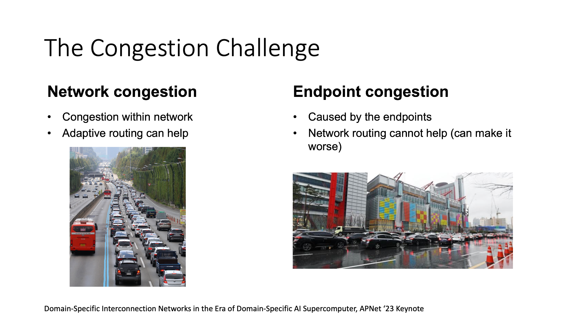
In response to the network challenges in AI, the mainstream solutions are through network congestion control or using flow control. The difference between these two methods is that flow control solves the congestion problem in the parking lot at the end, while congestion control solves the congestion problem on the road. If congestion control on the road is overly optimized, it may make the congestion problem in the parking lot at the end more serious.
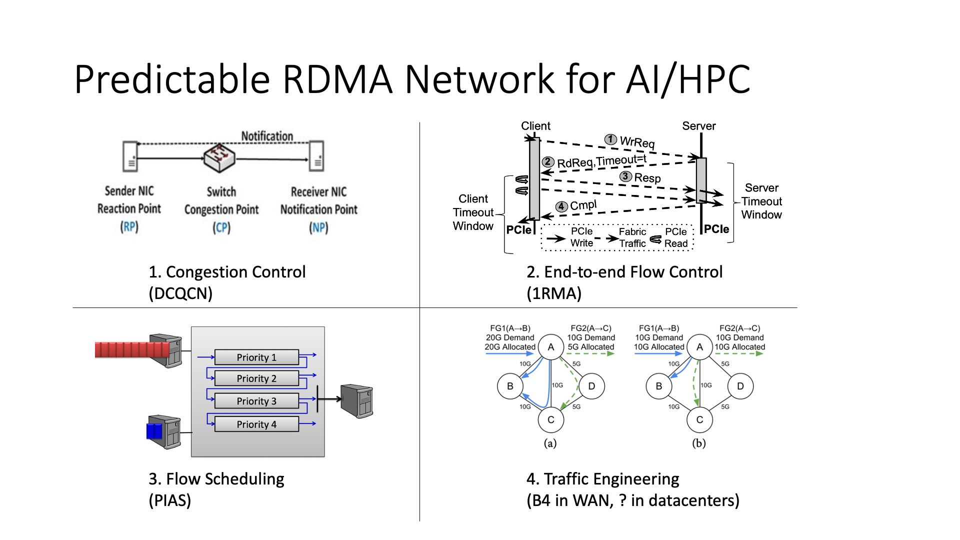
The workload of AI, especially large models like Transformer, has a good characteristic, that is, they are all very predictable.
Traditional congestion control and flow control are some reactive solutions, that is, when network congestion is discovered, then I will slow down.
A more advanced point, Flow Scheduling generally needs flow size information, and then it can prioritize the transmission of small flows, achieving the lowest FCT (Flow Completion Time).
The most extreme can be said to be Traffic Engineering, that is, planning in advance which flows need to be transmitted, calculating which route each flow takes, and fully utilizing the bandwidth of multiple routes in the network. Traffic engineering methods are mainly used in wide area networks, but few people use them in data centers, because people generally think that it is difficult to calculate the traffic in data centers in advance. But in AI, traffic can be estimated in advance, because before training, we know how big the tensor to be transmitted each time is.
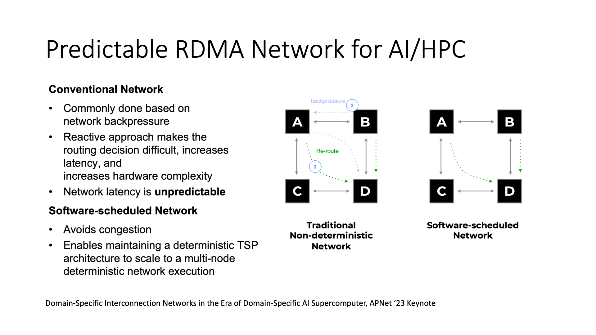
In AI workload, there are some new methods that can be used, such as software-scheduled networks. Traditional networks adjust after discovering congestion, such as adaptive routing or back-pressure. In software-defined networks, it may be possible to plan in advance which route each flow takes, so the efficiency of AI communication may be higher.
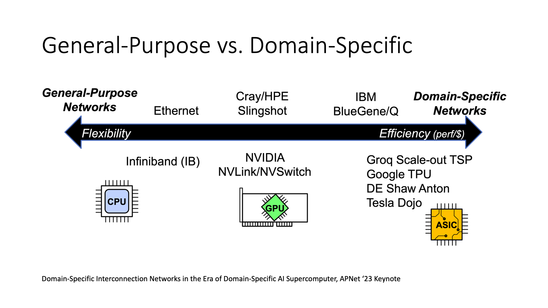
But this also raises a question, if the route of each flow is calculated in advance, is this network a general network or a dedicated network?
If I have planned everything, not only the planning at the software level, but also including its implementation in hardware, such as the current Groq, Dojo and other ASICs, it is a very dedicated network communication device. In this case, its efficiency will be higher because it is dedicated. The less efficient Ethernet, IB are general.
But there are also some in the middle state, such as NVIDIA’s products, which balance both generality and performance.
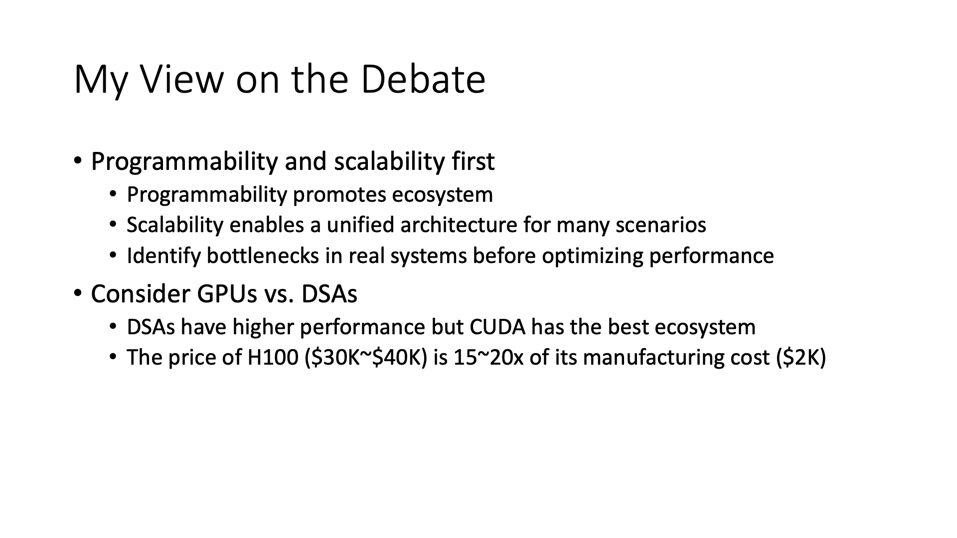
So should we make it general or dedicated? I personally think that it is not necessary to pursue the highest performance architecture, why? Just like the example of GPU and DSA, GPU is a product that NVIDIA has been promoting. It has a good ecosystem because it has put a lot of effort into developing this software ecosystem. However, DSA is definitely more efficient than GPU under the same chip process, possibly 50% higher, or even doubled.
But the problem is that programming DSA is very troublesome, often many operators are not supported, and development is difficult. So if the programming ability of this device is poor, the ecosystem may not be good, and finally this device may not sell well.
Another is the issue of scalability. The scalability here refers to whether it is scalable under large scale, such as IB cannot cross data centers, while RoCE can cross data centers. Another is the scalability of application scenarios.
For example, DSA, like Huawei’s Ascend, was originally customized for ResNet, because everyone was studying ResNet in 2016, but now the popular one is Transformer, which requires completely different things from ResNet, and the effective computing power of that chip is only 30%. So now there is a new version of Ascend, which can optimize Transformer a bit, so the effective computing power is 3 times higher than the previous generation of Ascend.
But during the development of the next generation of Ascend, NVIDIA has been selling GPU for several years. By the time the new generation of chips is fully deployed, and after two or three years, Transformer may not be popular anymore. So DSA architecture always has such a problem of generality.
In fact, the manufacturing cost of the chip is relatively low, such as H100, if I look at its manufacturing cost, it may be just 2000 US dollars, but in fact, it can sell for 30-40 thousand US dollars. If I make a chip, even if I sacrifice a bit of performance for generality, I can also make it a bit larger, with higher manufacturing costs and more power consumption. We can even use multiple chips to fight a chip, except for more power consumption, its performance can also be quite good, the entire profit space is actually still very large. So I think programmability and scalability are more important.
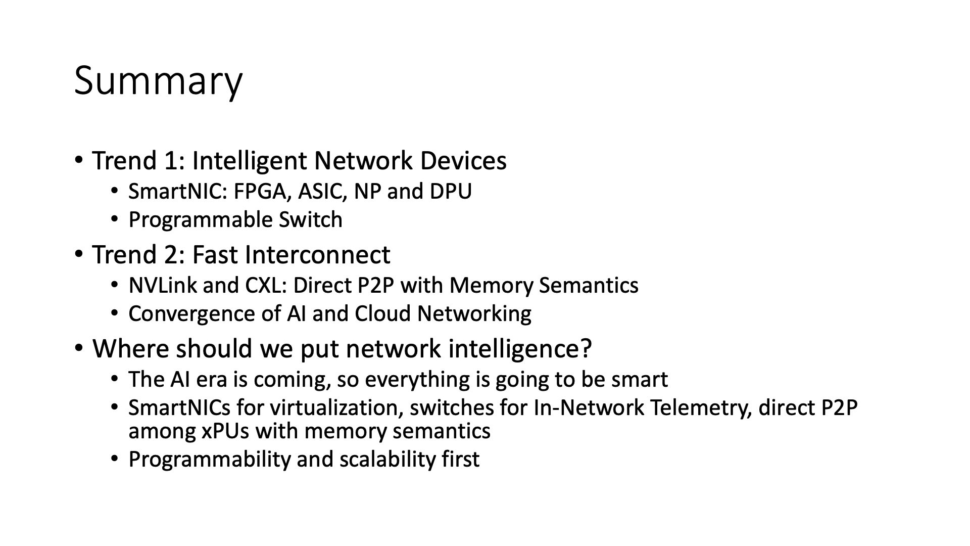
Finally, let’s make a simple summary. We have different architectures of smart NICs based on ASIC, NP, FPGA, and DPU, as well as programmable switches. At the same time, we also have high-performance interconnects based on memory semantics, such as NVLink and CXL can achieve point-to-point direct communication between devices, and integrate the interconnects inside and outside the host. In addition, AI and cloud computing are no longer independent clusters, but a unified computing platform that is integrated together.
Under such a general architecture, we can say that SmartNICs are mainly for virtualization, while switches may be more for allowing the system to perceive the network status and then make various real-time adjustments. If it is communication between GPU, NPU, and storage, because its efficiency needs to be very high, direct communication based on memory semantics may be the most suitable.
So there is an interesting point, that is, computing power can be placed anywhere, and there are different advantages in each place. The future is an AI world, and each computing device and network device may be very intelligent, so we just look at what kind of workload is more suitable to be placed where. Thank you all.

Thank you very much for Li Bojie’s sharing. If you have any questions, you can ask directly on Tencent Meeting.
Question 1: We mentioned GPU, so is NVSwitch across machines necessary?

Answer 1: In the training of models around 70B in size, the most critical is the communication in Tensor Parallelism. The communication in pipeline parallelism and data parallelism is not very large. For tensor parallelism, generally speaking, there is a high-performance NVLink interconnection between the 8 cards inside the host, which cannot be replaced by PCIe or RDMA. But for pipeline parallelism and data parallelism across machines, RDMA is enough.
But for larger models, such as GPT-4 models with thousands of B, 8 cards in a single machine for Tensor Parallelism are not enough, and NVLink interconnection across machines is needed. At present, the 256-card NVLink interconnection is basically enough. These 256 cards can basically be put into an enhanced rack, which is the so-called supernode, that is, the entire rack is made into a super high-speed interconnection, and the communication efficiency is like inside a node.
Question 2: What do you think about the multi-hosting in Alibaba’s CIPU architecture? Can multi-host reduce the failure rate?
Answer 2: If I only have one network card, I can virtualize it into two network cards, which is a way to reduce the cost of network cards. But the problem is that the failure domain has expanded. The failures of the two network cards of the two machines originally did not affect each other, but after virtualization, as long as this physical network card fails, both machines will not be able to access the network.
If two machines are virtualized into one machine, the problem is that its memory is not replicated, and I think this will increase the failure range. Originally my memory was local, but after doing this, part of the memory is stored locally and part is stored remotely. If the remote machine fails, there will be a problem.
Question 3: Now the bandwidth of the connection through NVLink is much wider than the bandwidth of PCIe, right?
Answer 3: Yes, definitely, because the fastest PCIe is now bidirectional 128G, and the bidirectional bandwidth of NVLink is 900G, which means its bandwidth is nearly 10 times that of PCIe.
Question 3: Are there any plans for me to design my own ASIC, not necessarily between CPUs, I am thinking if there is a design similar to SoC, the data sharing between CPU and CPU is through high-speed bus, that is, it has part of the memory can be moved by the GPU, will this cache be faster than RDMA?
Answer 3: It can be under certain scenarios. In fact, Huawei’s Unified Bus is doing this. It’s actually a bit like Apple’s Unified Memory. What it does is to use the same memory for CPU and GPU. Of course, because it’s a desktop, it might only have a communication bandwidth of 400 GB/s, right? It didn’t make it particularly high, but the server can make it higher, that is, it can make it to several hundred GB/s, right? Even up to TB/s is possible.

In essence, it’s the same as Nvidia’s Grace Hopper architecture. If you look at the architecture diagram of Grace Hopper, although the memory is not drawn in this diagram, we know that the memory is also shared. There is 144 TB of shared memory in it, and both CPU and GPU can directly connect to it. The communication bandwidth between CPU and GPU in it is also very high.
Question 3: The shared memory here actually also divides remote and near memory, right?
Answer 3: Yes, there is definitely a difference. For example, like a GPU, if it accesses its own memory, the efficiency is definitely the highest, because its bandwidth is 3.35 TB/s for example H100, but from the outside, it is actually just 900 GB/s or bidirectional, and the unidirectional is 450 GB/s, which is actually about 10 times less.
And when the GPU accesses memory, because it is parallel to fetch, the speed should be higher. But the number of CPU cores is relatively small, and there are not many outstanding memory requests in each core, it is actually serial. And there are Tensor Cores in the GPU, and a matrix is fetched at once, and the calculation efficiency is even higher.
Question 4: Yesterday, there was a discussion in a group about this issue. It’s about how NVIDIA is leading the trend in training acceleration, whether it’s for large models or otherwise. All things, including the design of the model itself, are done according to NVIDIA’s GPU and CUDA architecture. So, is it difficult to surpass NVIDIA in the industry? In fact, while you are working on something, you find that NVIDIA is working on something even more advanced. It’s hard to catch up with them in the short term. Then after a while, they have new updates, and they are in a continuous development process. Unlike CPUs, like Intel, Moore’s Law has already failed, and everyone can compete with them at some point.
Answer 4: I think it mainly depends on the issue of a customized architecture. For example, there are many DPUs now, which are actually customized by themselves. And things like Wafer-Scale Chips have super large bandwidth in the middle, which may be larger than NVLink, right? They are all in the TB range, and all the chips on the entire Wafer are directly connected, right? These are some newer architectures that can perform better than NVIDIA on some specific workloads.
But I think there is a core issue here, which is the co-evolution of models and hardware. As I said before, when we design models or set optimization goals, we will consider the execution efficiency of the model on the hardware. For example, the main goal of the designers of Transformer when designing was to improve efficiency. They didn’t overly pursue accuracy at the beginning, but focused on parallel computing, making its computing speed faster than traditional RNNs. Most of the models now are optimized for GPUs, so if the new architecture is not general enough, it is easy to fall behind the evolution of the model.

We talked about a 10-100-1000 rule before, where the 10 means that this workload should be able to be used for at least 10 years. If it’s too customized, it’s impossible to achieve this 10-year goal. So whether it’s Microsoft’s FPGA GFT offload, AWS Nitro’s flow table, or the flow table in NP and DPU, they all have a certain degree of generality and programmability, not just customized for the current virtualization needs of the cloud.

Question 5: Looking at this picture, the general architecture on the left is very flexible. The vertical design on the right is customized for future needs, which is more ideal. But compared with GPUs, although DSA has advantages in processing large models, it still has generality in many simulation calculations.
Answer 5: Yes, the general design on the left is undoubtedly feasible for high-performance computing (HPC). But the DSA design on the right is difficult to achieve high-performance computing, and its effective computing power will be greatly reduced. This is the problem with DSA.
Question 5: GPUs perform well when processing dense data, but when processing sparse matrices, such as sparse data calculations, the performance of Tensor Core is relatively poor.
Answer 5: Yes, the efficiency of sparse matrix calculation is indeed low. So now there are many researchers of FPGA and ASIC, they are all trying to accelerate on sparse and quantization.
I think it is very difficult for FPGA to surpass ASIC at present, because the efficiency of FPGA may be 10-100 times lower than that of ASIC for the same scale of logic. On the one hand, the frequency of FPGA is much lower than that of ASIC, on the other hand, each programmable gate in FPGA occupies several times the area of ASIC, which is the cost of programmability.
When we talked about the 10-100-1000 rule of FPGA offload before, 100 refers to 100 lines of C++ code. In 2015, the area of FPGA was very small and could not hold much logic. Today’s FPGA area is much larger, but it can only hold the logic of 1000 lines of C++ code. But as we said before, a complete RDMA implementation requires the level of 10000 lines of C code, which is unrealistic to put into FPGA completely, and can only put the hot path into it, which means that a small core must be set up next to FPGA for the cold path.
In fact, the ASIC Mellanox also does the same. We said before that RNR is a vulnerability that is easy to cause DoS attacks, because the error handling of RNR is executed on the firmware, not processed in the ASIC like the normal message path. But the area and power consumption of the same hot path in ASIC are much smaller than those in FPGA. So you see Mellanox’s network cards are all VPI cards, supporting both IB and RoCE, and a lot of acceleration capabilities. If you want to implement these logics in FPGA, you definitely can’t fit them.
In terms of DSA, I think it is a bit difficult to surpass GPU in quantization acceleration, because NVIDIA has done a lot of work in quantization, including the latest H100, etc., including the performance of 8 bit is already very high. But in sparse computing, I think NVIDIA’s work is relatively less, and the flops of sparse are only 2 times that of dense. If the proportion of 0 is really high, the performance is relatively poor. DSA has a lot of room for optimization.
In some earlier large model training and traditional AI algorithms such as recommendation systems, sparse computation occupies a relatively high proportion. However, if it is based on the current Transformer architecture, its proportion should not be high, because Transformers are all dense matrices. But if the future Transformer can become sparse, it may also have its significance.
But I think blindly pursuing sparsity may not necessarily be effective. The Pangu model made by Huawei earlier claimed to be a trillion-level model, equivalent to a model of thousands of B, but that model is sparse, that is, its actual parameter volume and computing power are far from reaching that high. Therefore, its final accuracy is not ideal. So the new version of the Pangu large model is based on the Transformer architecture and redone, and the accuracy has greatly improved than before.
If sparse computation is really important in the future, maybe NVIDIA will launch a sparse core as a supplement to the tensor core. We saw that in 2016, NVIDIA gave the first DGX-1 to OpenAI. They cooperated a long time ago, realized the importance of the tensor core, realized the importance of large-scale distributed training, and realized the importance of network bandwidth. Therefore, AI chip manufacturers must deeply cooperate with reliable large model companies to know what the future model looks like and what kind of computing power, storage, and communication are needed.
(End)